Structure of an optical interference display unit

a technology of optical interference and display unit, which is applied in the direction of television system, identification means, instruments, etc., can solve the problems of increasing the complexity of the process, and achieve the effects of improving the mechanical stress of the light absorbing layer, good uniformity and quality, and simplifying manufacturing steps

Inactive Publication Date: 2005-10-25
SNAPTRACK
View PDF5 Cites 229 Cited by
  • Summary
  • Abstract
  • Description
  • Claims
  • Application Information

AI Technical Summary

Benefits of technology

[0009]In the conventional manufacturing process of the optical interference display unit, an indium tin oxide (ITO) layer is formed on a transparent substrate, a metal light absorbing layer is formed on the ITO layer, and then a dielectric layer is formed on the metal light absorbing layer. Since there exists a large amount of hetero-atoms (such as oxygen, nitrogen, etc.) in both ITO and dielectric layer forming process, the metal absorbing layer must be formed in another reaction chamber thereby preventing contamination of the hetero-atoms. However, this increases the complexity of the process.
[0011]Another objective of the present invention is to provide an optical interference display unit wherein the light absorbing layer is disposed above the light-reflection electrode to prevent contamination of the hetero-atoms thereby achieving stable quality and high process yield.
[0012]Another objective of the present invention is to provide an optical interference display unit wherein the light-reflection electrode is comprised of a light absorbing layer and a light reflection layer such that the mechanical stress adjusting layer can be skipped to simplify the process, reduce costs and increase process yield.
[0018]However, in the optical interference display unit of the present invention, a sacrificial layer with a thickness of several micrometers to tens of micrometers is formed after the transparent conductive layer and the optical film are formed in sequence. Typically, the material of the sacrificial layer can be metal or silicon materials. The light absorbing layer is formed on the sacrificial layer and the supporters after the supporters are formed. Finally, the light reflection layer is formed. Since the sacrificial layer is thick enough to prevent contamination of the hetero-atoms generated in transparent conductive layer and optical film forming process, a light absorbing layer of very good uniformity and quality can be obtained even though the light absorbing layer has a thickness of only tens to hundreds of angstroms. Moreover, the sacrificial layer will be removed eventually thereby having no effect upon the light absorbing layer and the light reflection layer.
[0019]In addition, the mechanical stress of the light absorbing layer can be increased by adjusting the process parameters of the light absorbing layer forming step, e.g., reducing the applied power or the film-forming velocity in the metal deposition process. Therefore, the light absorbing layer can have the function of the mechanical stress adjusting layer that is optional in the present invention. The process parameters of the light absorbing layer forming step depend on the material and the thickness of the light reflection layer and the light absorbing layer.
[0020]The advantages of the optical interference display unit fabricated by the method provided in the present invention are listed as follows. Firstly, the manufacturing steps are simplified and the probable contamination is avoided such that the manufacturability of the optical interference display unit is increased and the resultant panel has a more stable characteristic and a better quality. Secondly, since the light absorbing layer can function as the mechanical stress adjusting layer, the mechanical stress adjusting layer is not required in practicing the present invention.

Problems solved by technology

However, this increases the complexity of the process.

Method used


Image

  • Structure of an optical interference display unit
  • Structure of an optical interference display unit
  • Structure of an optical interference display unit

Examples


example

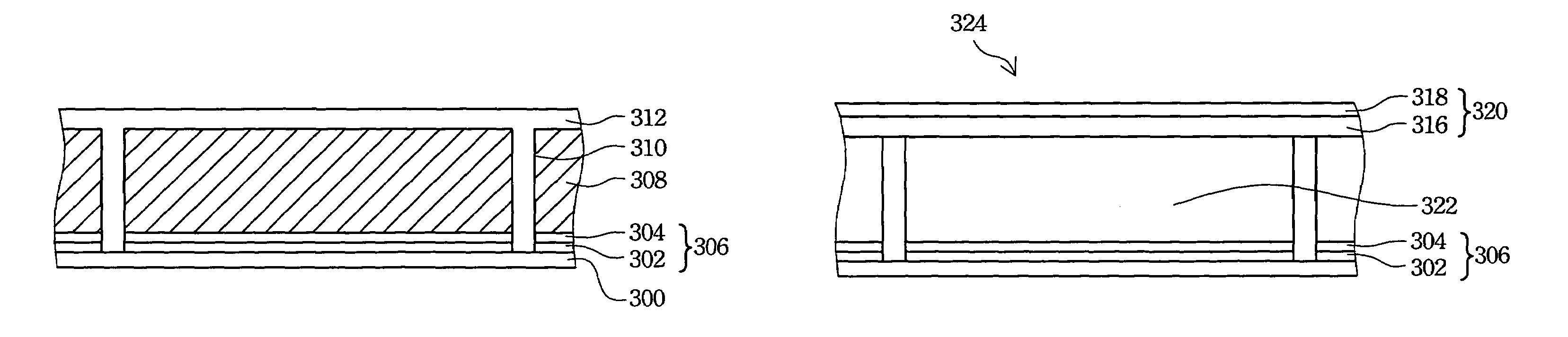
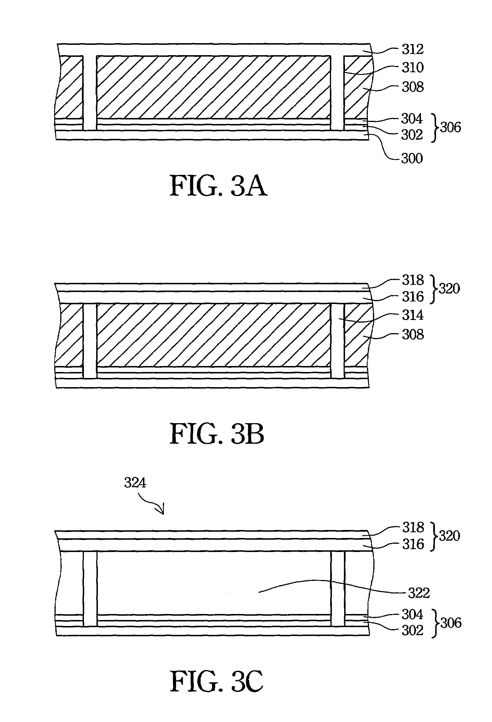
[0026]FIG. 3A to FIG. 3C illustrate a method for manufacturing an optical interference display unit in accordance with a preferred embodiment of the present invention. Referring to FIG. 3A, a transparent conductive layer 302 is formed on a transparent substrate 300. The material of the transparent conductive layer 302 can be indium tin oxide (ITO), indium-doped zinc oxide (IZO), zinc oxide (ZO), indium oxide (IO) or a mixture thereof. Thickness of the transparent conductive layer 302 is selected depending upon the requirement, but is typically tens to thousands of angstroms.

[0027]After the transparent conductive layer 302 is formed, at least one optical film 304 is formed on the transparent conductive layer 302. The material of the optical film 304 can be dielectric material such as silicon oxide, silicon nitride or metal oxide. The transparent conductive layer 302 and the optical film 304 constitute the light-reflection electrode 306. Then, a sacrificial layer 308 is formed on the ...


PUM

PropertyMeasurementUnit
transparentaaaaaaaaaa
thicknessaaaaaaaaaa
structureaaaaaaaaaa

Abstract

An optical interference display unit, at least comprises a light-incidence electrode and a light-reflection electrode located on a transparent substrate. The light-incidence electrode at least comprises a transparent conductive layer and a dielectric layer. The light-reflection electrode at least comprises an absorption layer and a reflective layer.

Description

FIELD OF INVENTION[0001]The present invention relates to an optical interference display panel, and more particularly, the present invention relates to a color changeable pixel unit for an optical interference display panel.BACKGROUND OF THE INVENTION[0002]Planar displays have great superiority in the portable display device and limited-space display market because they are lightweight and small. To date, in addition to liquid crystal displays (LCD), organic electro-luminescent displays (OLED), and plasma display panels (PDP), a mode of optical interference display is another option for planar displays.[0003]U.S. Pat. No. 5,835,255 discloses an array of optical interference display units of visible light that can be used as a planar display. Referring to FIG. 1, FIG. 1 illustrates a cross-sectional view of a conventional optical interference display unit. Every optical interference display unit 100 comprises a light-incidence electrode 102 and a light-reflection electrode 104 formed...

Claims


Application Information

Patent Timeline
Patent Type & Authority Patents(United States)
IPC IPC(8): G02B26/08G02B26/00G02F1/00G09F9/30H04N5/72G02F1/13G09F9/00
CPCG02B26/001G02B26/00
Inventor LIN, WEN-JIAN
Owner SNAPTRACK
Why Eureka
Try Eureka