Large EL panel and manufacturing method therefor

Inactive Publication Date: 2005-11-22
SEIKO EPSON CORP
View PDF27 Cites 30 Cited by
  • Summary
  • Abstract
  • Description
  • Claims
  • Application Information

AI Technical Summary

Benefits of technology

[0019]Each of the TFT layers has a pixel section and a circuit section. The pixel section is superimposed over the light emitting area, so that no problems occur. In contrast, however, the circuit section is disposed at the periphery, usually at two sides, of the TFT layer, and at the region outside the light emitting area. Accordingly, the circuit section prevents

Problems solved by technology

In the case in which a large display panel is formed by using the EL display devices, a problem has occurred that sub-transparent su

Method used


Image

  • Large EL panel and manufacturing method therefor
  • Large EL panel and manufacturing method therefor
  • Large EL panel and manufacturing method therefor

Examples


second embodiment

(Second Embodiment)

[0059]A second embodiment of the present invention will be described below. The components which are similar to those in the first embodiment are denoted by the same reference numerals, and descriptions thereof are omitted.

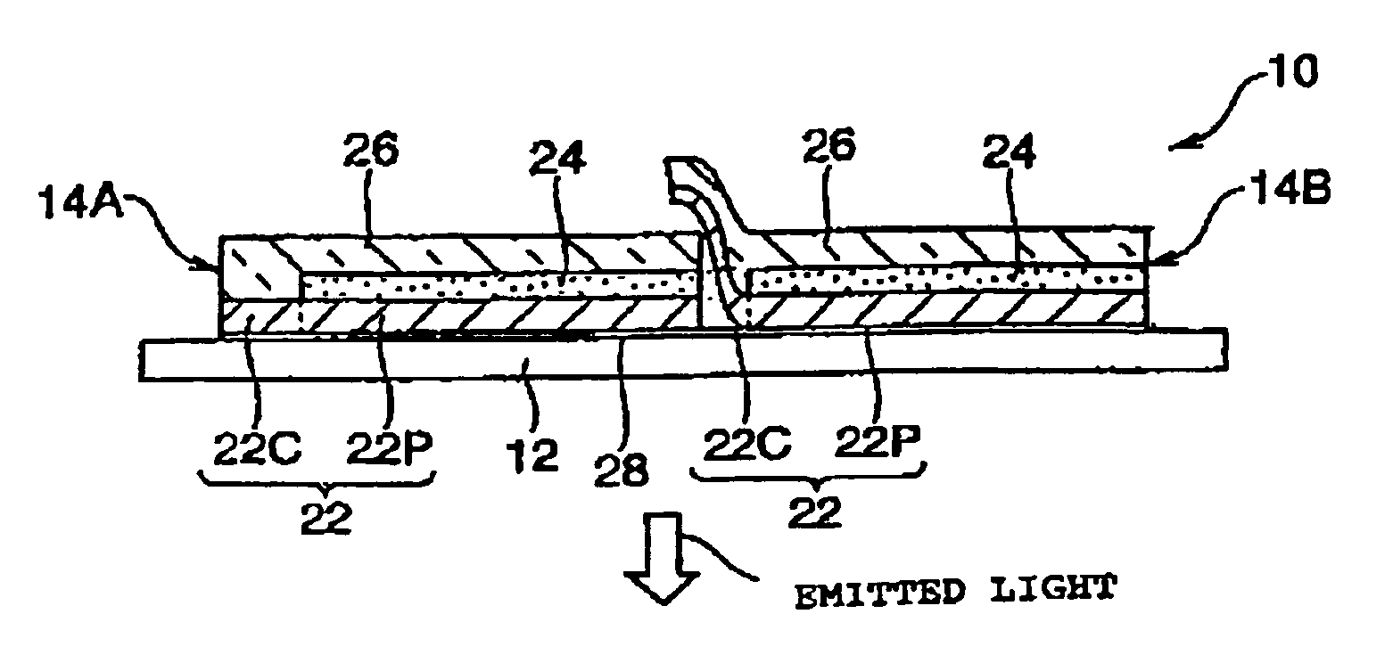
[0060]In the second embodiment, the circuit section 22C of the TFT layer 22 is disposed in a manner such that the TFT layer 22 is not bent at the boundary between the circuit section 22C and the pixel section 22P.

[0061]As shown in FIG. 9, the main transparent substrate 12 is provided with a step portion 30 formed by the adhesive layer 28 which is used for laminating and fixing the EL display devices 14. The step portion 30 is provided so as to change the positions of adjacent EL display devices 14 in the thickness direction.

[0062]The height of the step portion 30 corresponds to the total thickness of the TFT layer 22 and the base layer 24. Accordingly, the circuit section 22C may be disposed behind the adjacent EL display device 14 without bendi...

third embodiment

(Third Embodiment)

[0063]A third embodiment of the present invention will be described below. The components which are similar to those in the first embodiment are denoted by the same reference numerals, and descriptions thereof are omitted.

[0064]In the third embodiment, the circuit section 22C of the TFT layer 22 is also disposed in a manner such that the TFT layer 22 is not bent at the boundary between the circuit section 22C and the pixel section 22P.

[0065]As shown in FIG. 10, in the third embodiment, the transparent electrode layer (not shown) is laminated on the main transparent substrate 12 as a first layer. In addition, the base layer 24 is provided as a second layer, and the TFT layer 22 is provided as a third layer. Accordingly, the transparent electrode layer, the base layer 24, and the TFT layer 22 are laminated inversely compared to the manner in the first and the second embodiment. In addition, the thickness of the pixel section 22P of the TFT layer 22 is double compared...

fourth embodiment

(Fourth Embodiment)

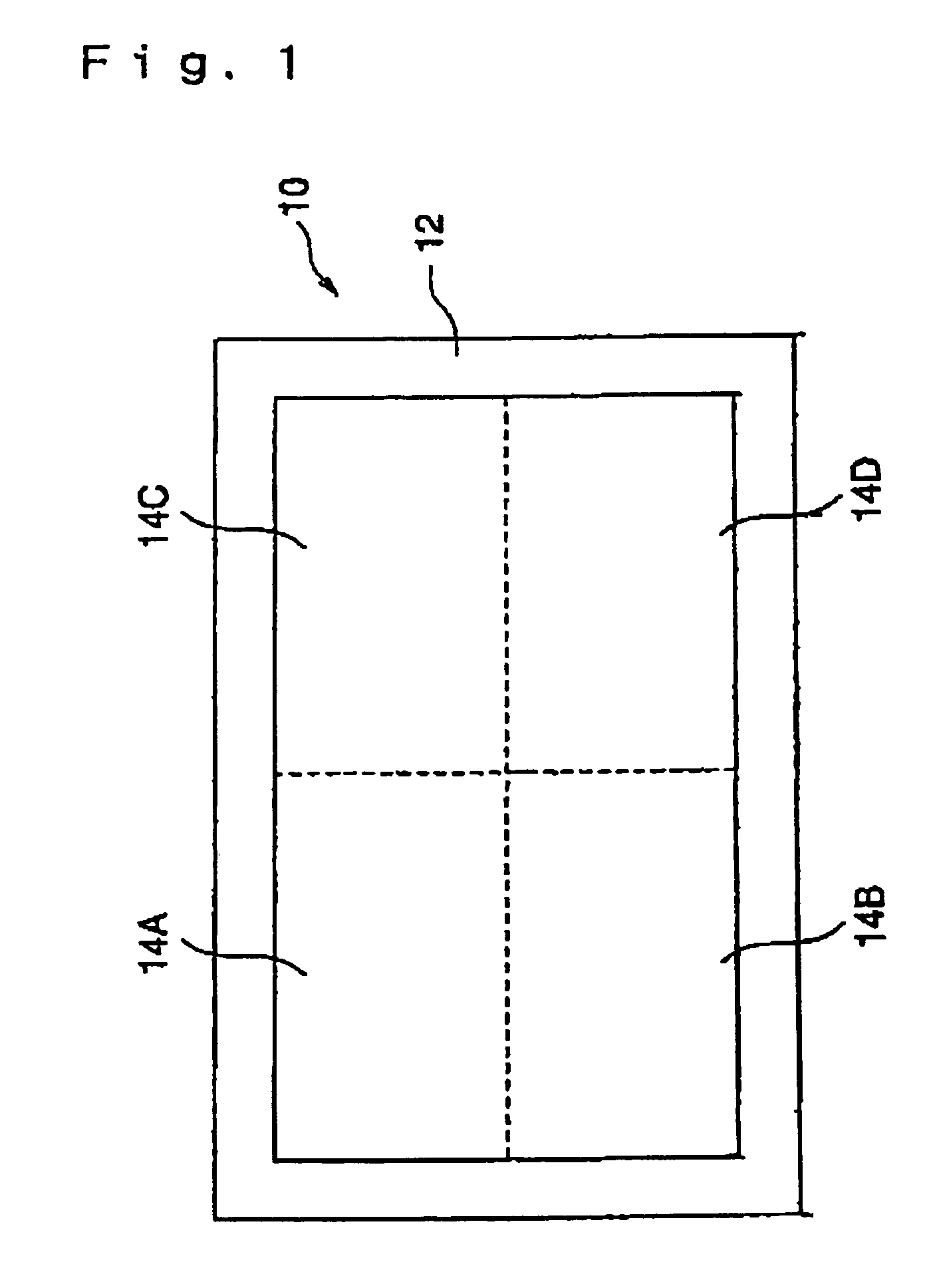
[0068]The following embodiment may only be applied when four EL display devices 14 are provided. FIG. 11 shows a first modification in which the four EL display devices 14 are arranged in proximity to each other. In this case, four similar EL display devices 14 are prepared, and the two EL display devices 14 disposed in the right side and the two EL display devices 14 disposed in left side are arranged inversely to each other. Accordingly, the circuit sections 22C of the TFT layers 22 are prevented from overlapping on the adjacent EL display devices 14.


PUM


Abstract

A manufacturing method is disclosed for a large EL panel in which a plurality of EL display panels are used. Each of said plurality of EL display panels are constructed of an EL display device and a sub-transparent substrate. The EL display device includes a base layer over which a luminescent material is applied, an electrode layer which is laminated on one side of said base layer, and a TFT layer including a circuit section. The circuit section of a TFT layer is disposed behind an adjacent EL display device. Thus, the EL display devices appear to be unified, forming a large EL display panel. In addition, in the case of in which a plurality of EL display devices are arranged in a matrix pattern, pitch between the pixels provided in the pixel section of the TFT array is maintained constant.

Description

[0001]This is a Division of Application Ser. No. 09 / 856,852 filed May 29, 2001. The entire disclosure of the prior application is hereby incorporated by reference herein in its entirety.BACKGROUND OF THE INVENTION[0002]1. Field of the Invention[0003]The present invention relates to a large EL panel formed by a plurality of EL display devices, such as organic EL panels, which are arranged in a matrix pattern, and also relates to a manufacturing method for the large EL panel.[0004]2. Description of the Related Art[0005]Small EL flat panels (EL display devices) driven by polysilicon TFTs are usually laminated on a hard and transparent substrate by an adhesive, etc., in order to maintain the flatness thereof. Each of the TFTs control the driving of one of multiple pixels in the EL display devices, so that plane images are displayed.[0006]The EL display devices as described above are typically two to six inches in length measured in a diagonal direction, and provide excellent functions a...

Claims


Application Information

Patent Timeline
IPC IPC(8): G09F9/313G09F9/30G09F9/40H01L27/32H01L51/50H05B33/12H05B33/14
CPCG09F9/313H01L27/3293H01L27/3244H10K59/18H10K59/12H05B33/00
Inventor SHIMODA, TATSUYANISHIKAWA, TAKAO
Owner SEIKO EPSON CORP
Why Eureka
Try Eureka