

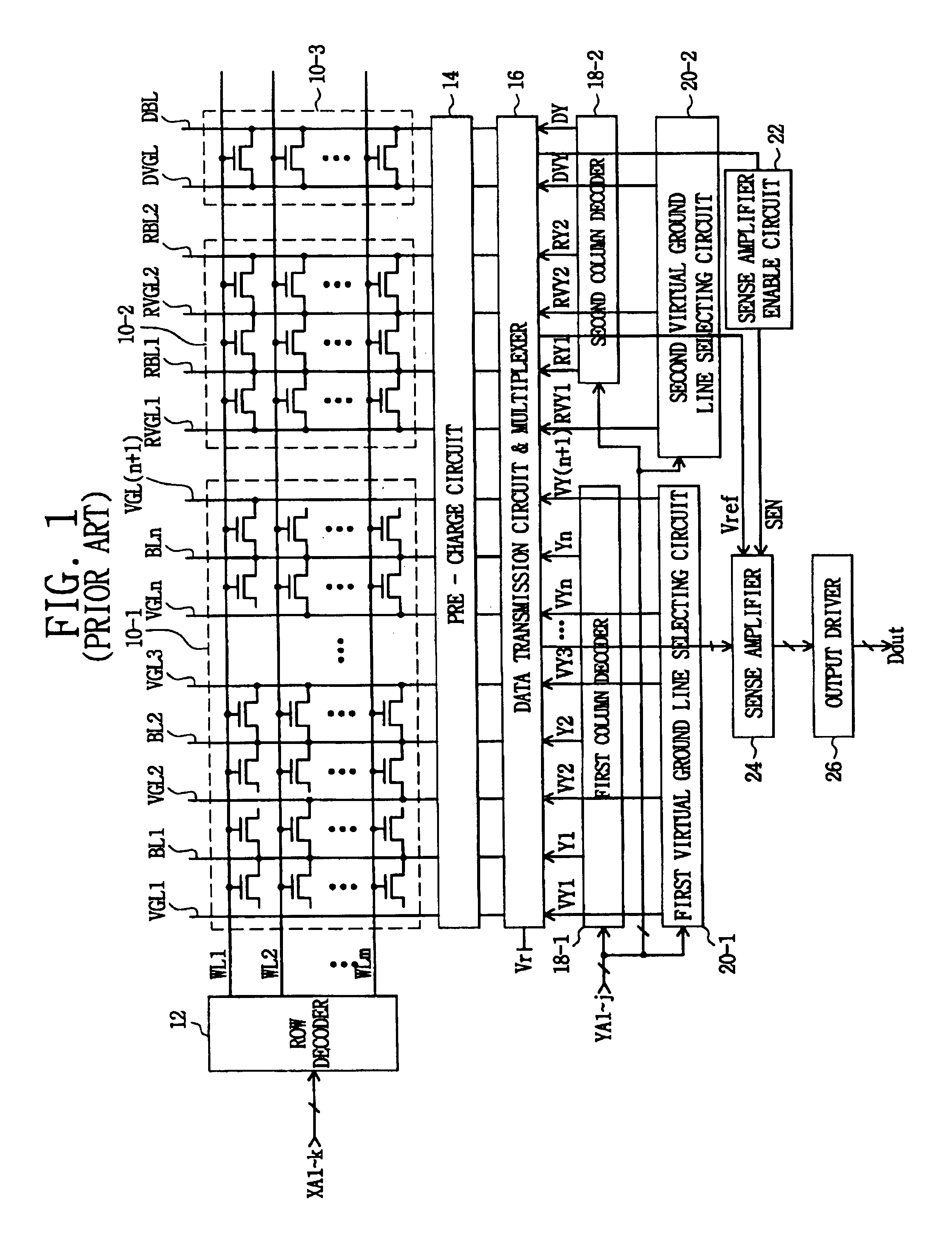
Read only memory device
a memory device and read only technology, applied in the field of memory devices, can solve problems such as higher data read errors
- Summary
- Abstract
- Description
- Claims
- Application Information
AI Technical Summary
Benefits of technology
Problems solved by technology
Method used
Image

Examples
first embodiment
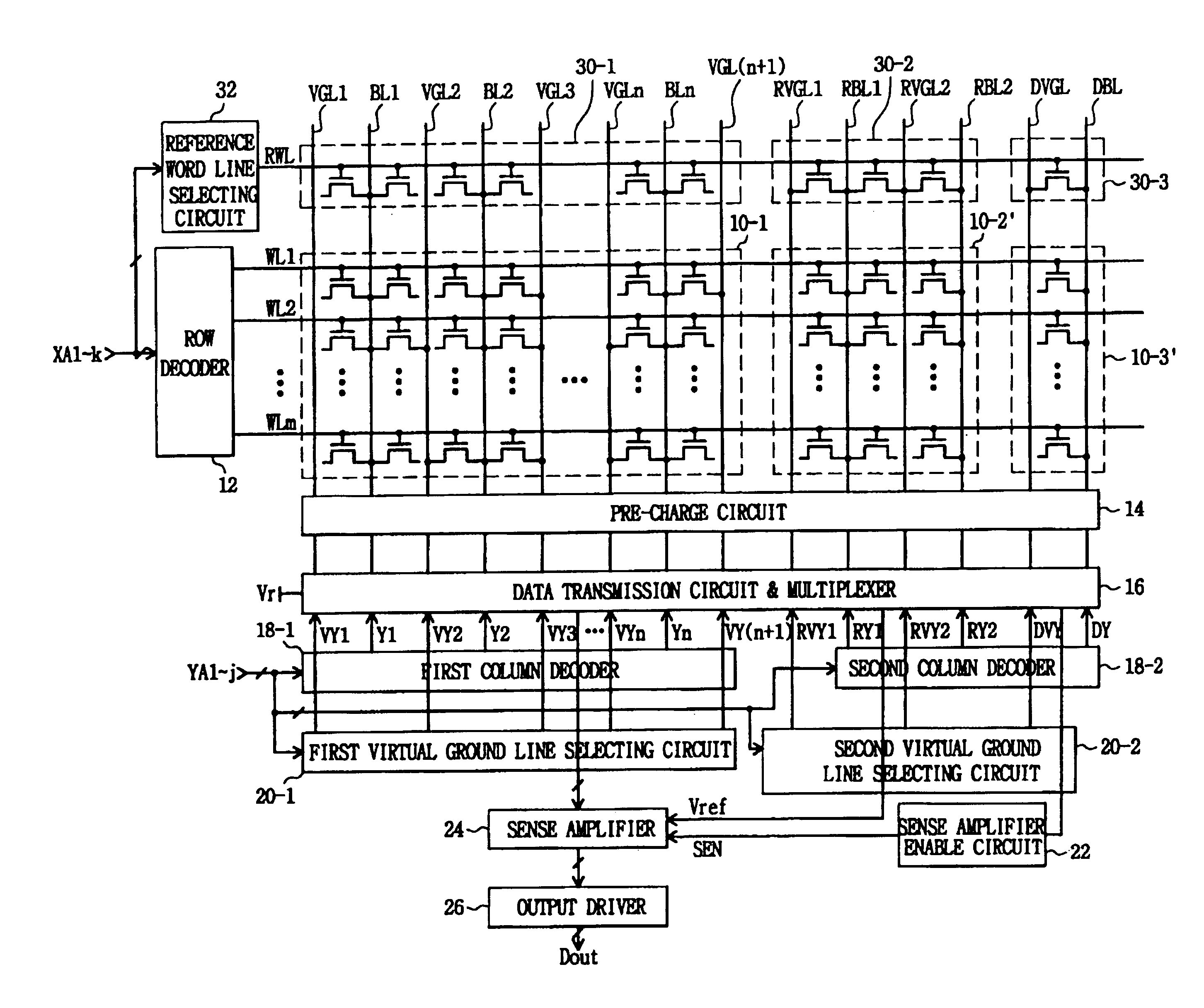
[0040]FIG. 3 is a block diagram illustrating a read only memory device of the present invention. The read only memory device of FIG. 3 includes second read only memory cells 30-1, second reference memory cells 30-2, a second dummy memory cell 30-3, and a reference word line selecting circuit 32 in addition to the configuration of the read only memory device shown in FIG. 1.
[0041]In FIG. 3, the second read only memory cells 30-1 are programmed to a logic high (e.g., data “1”) between the reference word line RWL, the bit lines BL1 to BLn, and the virtual ground lines VGL1 to VGL(n+1). The second reference memory cells 30-2 are programmed to a logic low (e.g., data “0”) between the reference word line RWL, the reference bit lines RBL1 and RBL2, and the reference virtual ground lines RVGL1 and RVGL2. The second dummy memory cell 30-3 are programmed to a logic low (e.g., data “0”) between the reference word line RWL, the dummy bit line DBL and the dummy virtual ground line DVGL.
[0042]Tha...
second embodiment
[0051]FIG. 4 is a block diagram illustrating a read only memory device of the present invention. The read only memory device of FIG. 4 has the same configuration of that of FIG. 3 except that a level of a ground voltage VSS is applied to the word lines of the first reference memory cells 10-2′ and the first dummy memory cells 10-3′.
[0052]That is, the reference word line RWL and the dummy word lines DWL1 to DWLm are not connected to the word lines WL1 to WLm of the first read only memory cells 10-1 and is configured such that a ground voltage VSS level is applied thereto.
[0053]The read only memory device of FIG. 4 operates similarly to the device of FIG. 3.
[0054]FIG. 5 is a block diagram illustrating a third embodiment of a read only memory device of the present invention. The read only memory device of FIG. 5 has the same configuration of that of FIG. 3 except that the second bit lines and the virtual ground lines (i.e., second virtual ground lines) of the second read only memory ce...
PUM
 Abstract
Description
Claims
Application Information