Intermediate substrate

a technology of intermediate substrates and substrates, applied in the field of intermediate substrates, can solve the problems of increasing the number of terminals, difficult to form fine wiring patterns with high integration, and the overall height of the substrate connection structure is reduced, and the number of connection steps is reduced.

Active Publication Date: 2005-12-27
NGK SPARK PLUG CO LTD
View PDF9 Cites 70 Cited by
  • Summary
  • Abstract
  • Description
  • Claims
  • Application Information

AI Technical Summary

Benefits of technology

[0009]It is hence an object of the invention to provide an intermediate substrate which is substantially immune from disconnection by thermal stress, which lowers overall height of the substrate connection structure, and which reduces the number of connection steps.

Problems solved by technology

If there is a substantial gap between the IC side terminal interval and the terminal interval at the main substrate (mother board) side at the point of connection, the wiring and via disposition pattern for providing the necessary conversion tends to be both fine (very dense) and complex.
Further, an additional problem is presented by the increase in the number of terminals.
), and the main substrate (having a coefficient of linear expansion of, for example, 17 to 18 ppm / ° C.) cannot be accommodated, and thus may lead to disconnection caused by solder peeling and / or other defects.
However, because, in the ceramic package substrate, the wiring is provided by printing and baking a metal paste, it is hard to form fine wiring patterns with high integration, in contrast to organic package substrates which are formed using photolithography technology.
Thus, the ceramic package substrate is limited in its ability to reduce the terminal interval at the semiconductor integrated circuit device side.
This is a serious disadvantage because of the current demand for size reduction.

Method used


Image

  • Intermediate substrate
  • Intermediate substrate
  • Intermediate substrate

Examples


Embodiment Construction

[0041]Referring now to the drawings, preferred embodiments of the invention will now be specifically described in connection with these drawings.

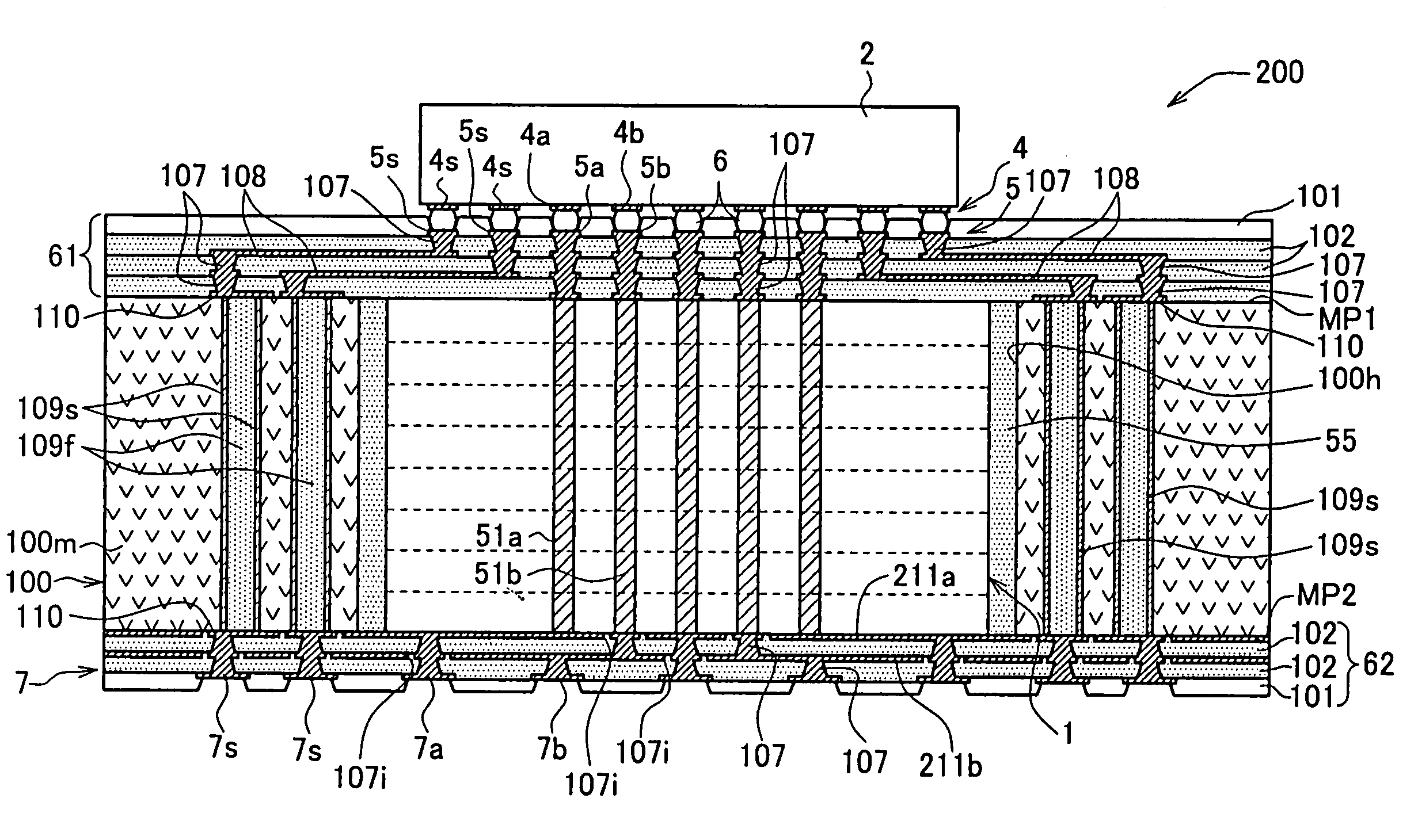
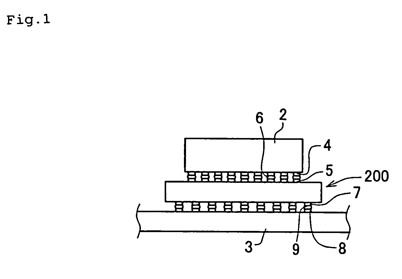
[0042]FIG. 1 shows an example of an intermediate substrate 200 in accordance with one embodiment of the invention disposed between a semiconductor integrated circuit device 2 and a main substrate 3. In this embodiment, a first principal surface of a plate member is exposed at the upper side as viewed in FIG. 1, and a second principal surface is exposed at the lower side.

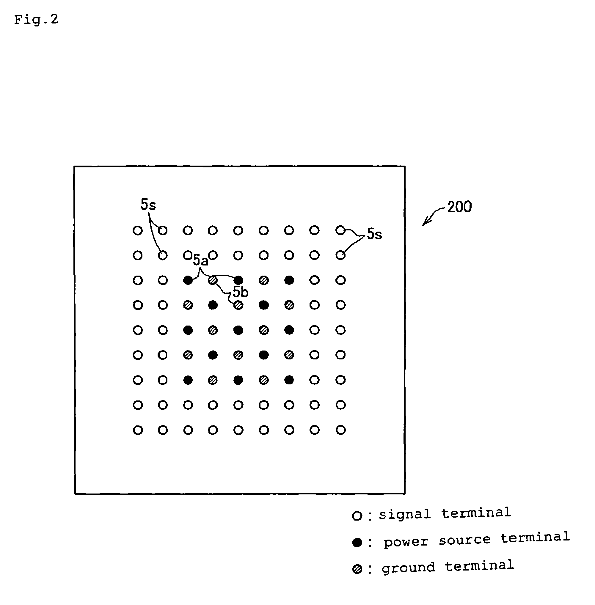
[0043]The semiconductor integrated circuit device 2 has a device side terminal array 4 comprised of a plurality of signal terminals, power source terminals, and ground terminals on the second principal surface, and is connected to a first terminal array 5 formed on the first principal surface of an intermediate substrate 200, by a flip-chip connection, by means of a solder junction 6. The main substrate 3 preferably comprises a mother board, or an organic laminated package s...


PUM

PropertyMeasurementUnit
temperatureaaaaaaaaaa

Abstract

An intermediate substrate is provided which reduces the effect of the difference in the coefficients of linear expansion between the terminals of the substrate and those of a semiconductor integrated circuit device, and which thus lowers the likelihood of disconnection due to thermal stress. The intermediate substrate, which is a planar member made of a polymeric material, includes a substrate core including a main core body having formed therein a sub-core compartment, and a ceramic sub-core section accommodated in the compartment. A first terminal array on the first principal surface side includes two types of terminals, functioning either as power source terminals or ground terminals, and a signal terminal. The array occupies an area entirely included within an orthogonally projected region of the sub-core section projected onto a reference plane parallel to the planar surface of the substrate core.

Description

BACKGROUND OF THE INVENTION[0001]1. Field of the Invention[0002]The present invention relates to an intermediate substrate and, more particularly, to an intermediate substrate for a semiconductor integrated circuit device.[0003]2. Description of the Related Art[0004]Semiconductor integrated circuit devices operating at high speeds, such as CPUs and other LSIs, have been much reduced in size in recent years, whereas the number of signal terminals, power source terminals and ground terminals has been increasing, and the terminal interval, i.e., the spacing between terminals, is becoming smaller or narrower. A terminal array on the integrated circuit side, which is typically comprised of packed multiple terminals, is generally connected to the mother board side of a flip-chip form, but because the terminal interval of the integrated circuit side terminal is significantly different from that of the mother board side terminal array, an intermediate substrate is required to accommodate th...

Claims


Application Information

Patent Timeline
Patent Type & Authority Patents(United States)
IPC IPC(8): H01F5/00H01L23/02H01L23/12H01L23/498H01L23/50H05K1/11H05K3/46
CPCH01L23/49822H01L23/49838H01L23/50H05K3/4602H05K3/4694H01L23/49827H01L2224/16235H01L23/49833H01L2224/16H01L2924/01012H01L2924/01025H01L2924/01078H01L2924/09701H01L2924/15174H01L2924/15311H01L2924/3011H05K1/112H05K2201/0187H05K2201/10674H01L2924/01019H01L2224/05573H01L2224/05568H01L2924/00014H01L2224/16225H01L2224/06131H01L2224/05599
Inventor KAMBE, ROKUROKASIWAGI, TETSUYAKIMURA, YUKIHIROSUGIMOTO, YASUHIROSUZUKI, KAZUHIRO
Owner NGK SPARK PLUG CO LTD
Why Eureka
Try Eureka