Manufacturing process for ultra slim electrooptic display device unit

a manufacturing process and electrooptic technology, applied in the direction of optics, identification means, instruments, etc., can solve the problems of increasing manufacturing man-hours, easy to have problems with picture quality and reliability, and affecting the quality of the device, so as to achieve low electric current leakage qualities, high electron and positive hole mobility, and low cost

Inactive Publication Date: 2006-01-03
SONY CORP
View PDF9 Cites 84 Cited by
  • Summary
  • Abstract
  • Description
  • Claims
  • Application Information

AI Technical Summary

Problems solved by technology

Because of this, the device quality and especially high speed operational characteristics become a problem.
However, with LCOS, it is easy to have problems with picture quality and with reliability resulting from TFT leak electric current due to strong incident light.
As a result, there is an increase in manufacturing man-hours, and a yield and production decrease due to the light leakage issue.
Although we can think of adopting a SOI (Silicon on Insulator) substrate (for instance, please see the patent document 1˜6) a monocrystalline Si substrate does not achieve optical transparency in this case.
However, in case where a transmissive LCD which is composed of the peripheral circuitry and the image element display on the surface of a monocrystalline Si substrate such as described in the patent document 7 is used in a unit such as a projector that reflects strong light, the monocrystalline Si substrate has high electron and positive hole mobility and very high sensitivity which causes a problem with TFT current leakage when exposed to strong incident light.
Even with a high intensity reflective LCD such as recent LCOS types, a problem with TFT current leakage of the display caused by strong incident radiation can be a problem.

Method used


Image

  • Manufacturing process for ultra slim electrooptic display device unit
  • Manufacturing process for ultra slim electrooptic display device unit
  • Manufacturing process for ultra slim electrooptic display device unit

Examples


Embodiment Construction

[0333]An execution form of the present invention will be described in detail below with reference to the accompanying diagrams for better understanding of the present invention.

[0334](A) A Method of Separating a Porous Semiconductor Layer

[0335](A-1) Ultra Slim Transmissive Type LCD

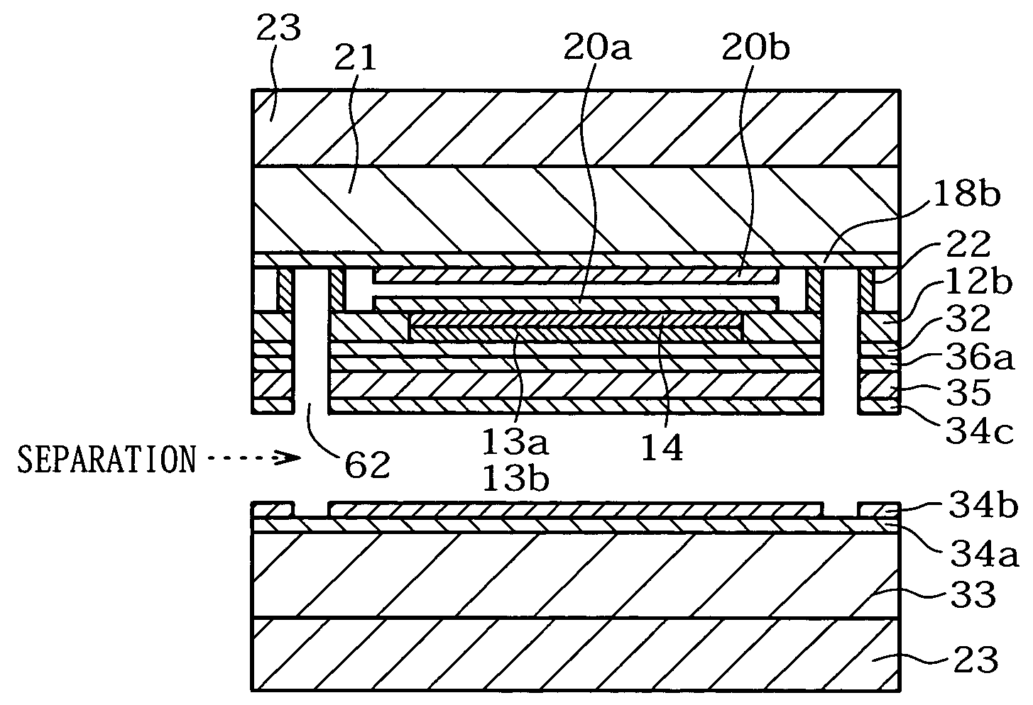
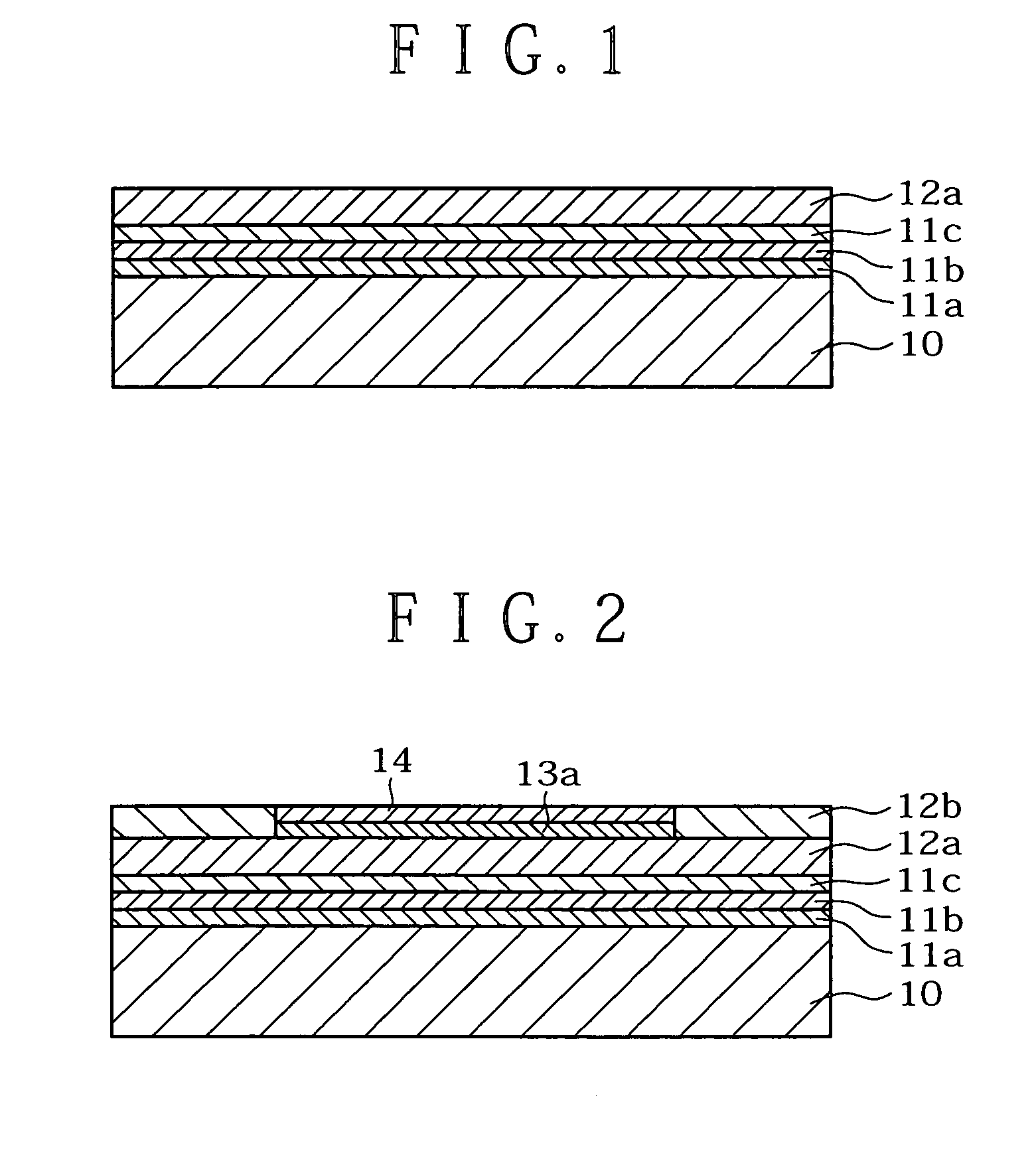
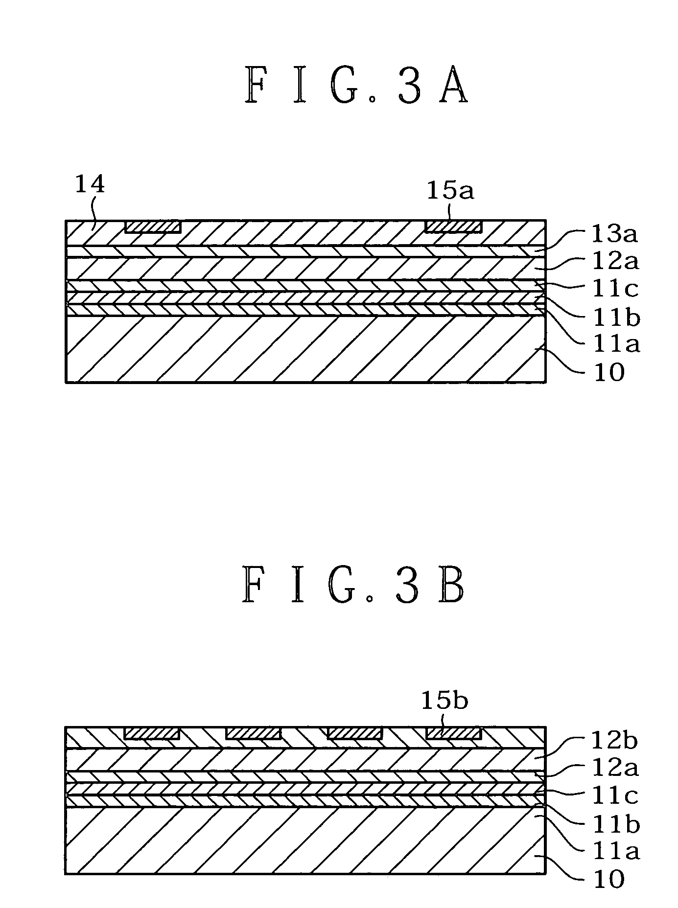
[0336]In this execution form, a method of producing an ultra slim electrooptic display by separation of a porous semiconductor layer using a porous silicon layer (hereafter referred to as “Si”) is described. FIG. 1 through FIG. 16 are process diagrams for manufacturing an ultra slim LCD by separation of a porous Si layer in the preferred execution form of the present invention.

[0337](1) Porous Si layers (11a: low porous Si layer, 11b: high porous Si layer, 11c: low porous Si layer) are formed by anodic oxidation on a monocrystalline Si substrate 10 as a support substrate.

[0338][1] Initially, p-type impurities are added in an approximately boron density of 1×10¹⁹ atoms / cm3 by a CVD method using monosilane g...


PUM

PropertyMeasurementUnit
insulatingaaaaaaaaaa
semiconductoraaaaaaaaaa
depthaaaaaaaaaa

Abstract

To obtain a high intensity, high definition and sophisticated electrooptic display device unit such as transmissive type LCD, a semi-transmissive type LCD, a reflective type LCD, a surface emitter type organic EL, or an underside emitter type organic EL, etc. which has high electron and positive hole mobility and low leak electric current qualities.A porous semiconductor layer (low porous Si layer 11a / high porous Si layer 11b / low porous Si layer 11c), a monocrystalline Si layer12a, and the Si O2 layer 13a are formed on a monocrystalline Si substrate 10. The Si O2 layer 13a of the peripheral circuit area is removed, leaving the Si O2 layer 13a in the display area. The poly Si layer 14a is formed in the display area by semiconductor epitaxial growth, and a monocrystalline Si layer 12b is formed in the peripheral circuit area. Then, the display element section is formed in the poly Si layer 14 of the display area and the peripheral circuitry section is formed in the monocrystalline Si layer 12b of the peripheral circuit area. The assembly is divided into each ultra slim electrooptic display device unit after separation from the backing, and after the process of separating the Si substrate 10 from the porous Si layer 11b and by attaching the backing to the ultra slim electrooptic display element substrate after its separation. Each ultra slim electrooptic display device unit is divided after attaching the backing.

Description

[0001]The present application claims priority to Japanese Patent Application JP2003-083056, filed in the Japanese Patent Office on Mar. 25, 2003; and Japanese Patent Application JP2004-024897, filed in the Japanese Patent Office on Jan. 30, 2004, the entire contents of which are incorporated herein by reference.BACKGROUND OF THE INVENTION[0002]1. Field of the Invention[0003]This invention relates to the manufacturing process for ultra slim electrooptic display device units such as high intensity, high definition and sophisticated transmissive liquid crystal display device units (LCD; Liquid Crystal Display), semi-transmissive liquid crystal display device units, highly reflective liquid crystal display device units, top surface luminous organic EL (Electro Luminescence) display device units and under surface luminous organic EL display device units.[0004]2. Description of Related Art[0005]In the case of a transmissive, high temperature polycrystalline silicon (which we will call “Po...

Claims


Application Information

Patent Timeline
Patent Type & Authority Patents(United States)
IPC IPC(8): H01L21/00H01L21/30G02F1/13H01L21/20G02F1/1362G09F9/00H01L21/02H01L21/336H01L27/12H01L29/786
CPCG02F1/136277G02F1/13454G02F2202/105G02F2202/104H04M1/0216
Inventor HIDEO, YAMANAKA
Owner SONY CORP
Why Eureka
Try Eureka