Automatic defect classification with invariant core classes

a defect classification and core class technology, applied in the direction of instruments, using wave/particle radiation means, semiconductor/solid-state device testing/measurement, etc., can solve the problems of low manufacturing yield, reduced production throughput, and large undetected defects, and achieve automatic, fast and reliable defect classification.

Inactive Publication Date: 2006-01-17
APPLIED MATERIALS INC
View PDF21 Cites 54 Cited by
  • Summary
  • Abstract
  • Description
  • Claims
  • Application Information

AI Technical Summary

Benefits of technology

[0014]An object of the present invention is to provide a method and apparatus for automatic, fast and reliable classification of defects in semiconductor wafers.

Problems solved by technology

As a result, such defects remain largely undetected until a considerable number of wafers have been fabricated and have begun to exhibit problems caused by the defects.
This late discovery of defects can result in a low manufacturing yield and reduced production throughput.
Furthermore, because the defects are not classified until an alarm is raised, and the alarm indicates only that a certain number of defects has probably occurred, alarms may also be generated when only an acceptably small amount of defects of a serious type have occurred; i.e., there is no way to determine before the alarm is raised whether the potential defects are likely to warrant corrective action.
Moreover, optical devices such as CCDs are limited in their ability to analyze and accurately identify defect types.
Firstly, the resolution of their images is limited by the pixel size.
Secondly, since they produce only two-dimensional images, they cannot gather a large amount of information regarding the topography of a defect, or whether it lies on the surface or below the surface of the wafer.
Thirdly, brightness due to reflection of light from certain types of defects, such as scratches, overwhelms the CCD and may produce false defect counts and false alarms.
However, the efficiency of these methods is reduced because there is no agreed-upon set of defect classes.
Another problem with prior art defect classification systems is that, because they are tailored to user-specific classes, they require many examples of defect images to be obtained for each defect class prior to becoming operational.
Consequently, prior art systems cannot be used during start-up and ramp-up of a production line.

Method used


Image

  • Automatic defect classification with invariant core classes
  • Automatic defect classification with invariant core classes
  • Automatic defect classification with invariant core classes

Examples


Embodiment Construction

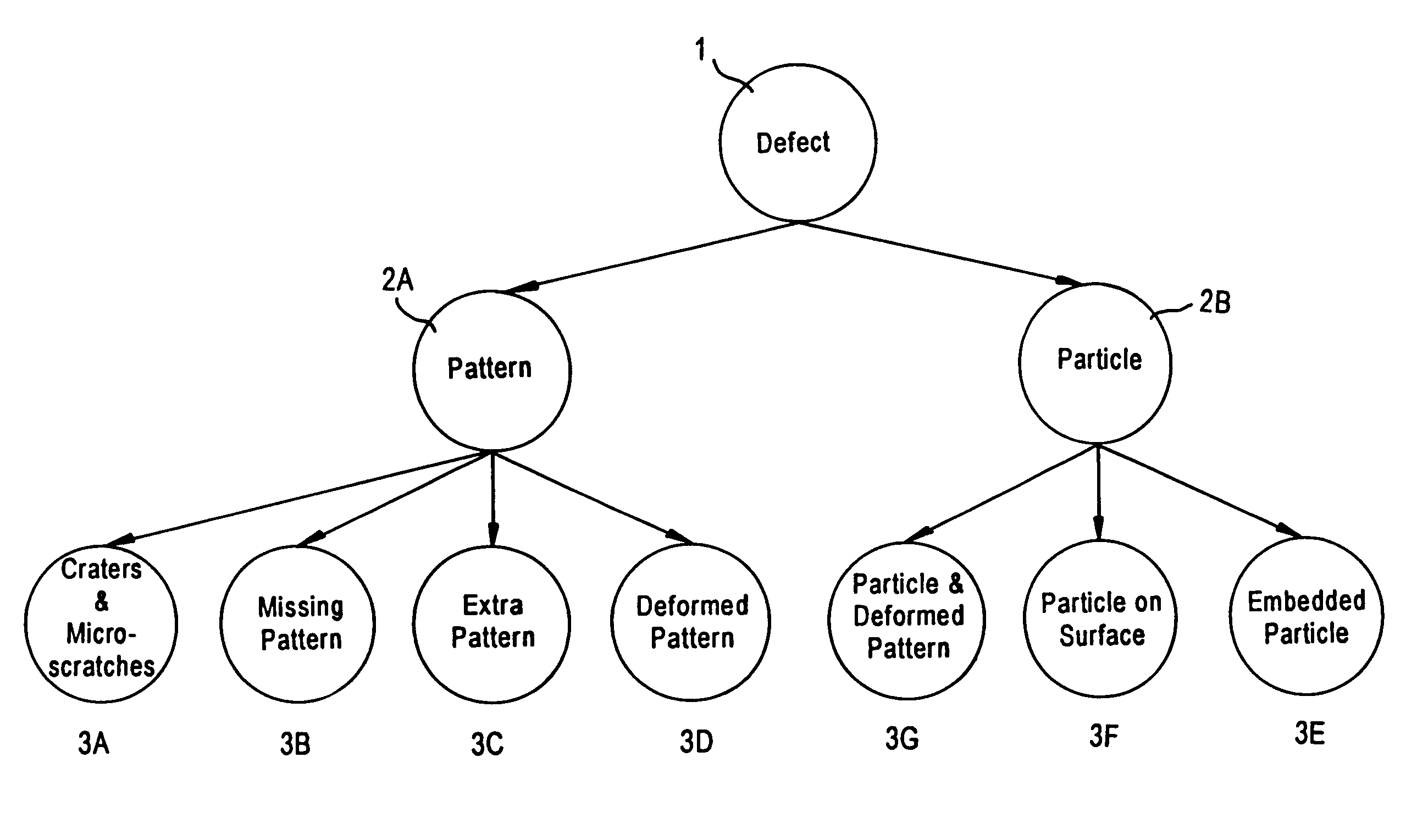
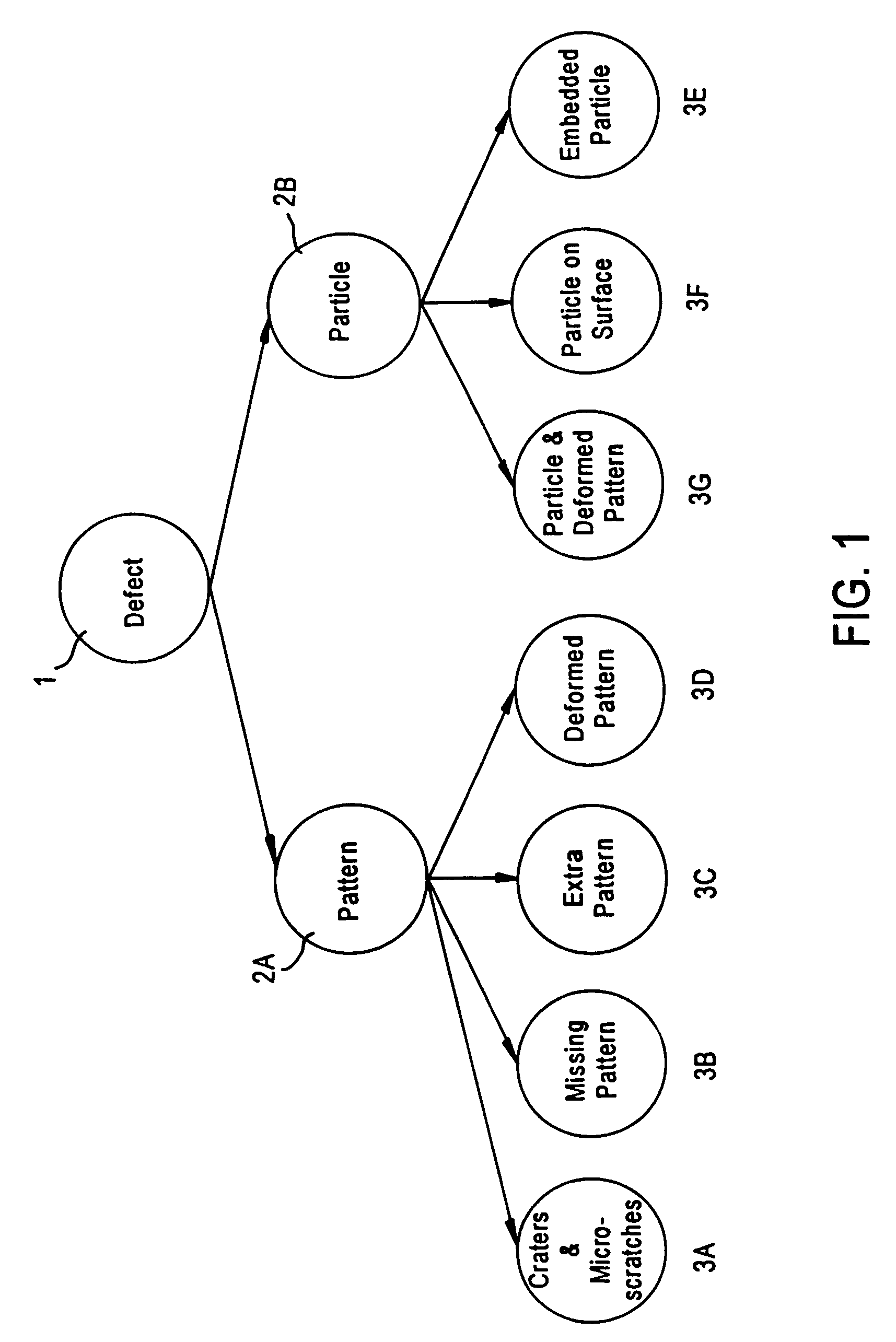
[0038]Conventional semiconductor wafer inspection techniques do not provide early detection of serious defects, but rather only indicate that a certain amount of defects of all types have occurred. Furthermore, conventional inspection techniques are not capable of analyzing defects in sufficient detail to provide information which leads to early positive identification of the defect source. The present invention addresses and solves these problems by providing automatic classification of defects into meaningful categories, enabling ready identification of processes causing defects, and enabling early corrective action to be taken.

[0039]According to certain embodiments of the methodology of the present invention, after a defect map of a semiconductor wafer has been generated, each defect site and a corresponding known non-defective reference site is imaged by a scanning electron microscope (SEM) to gather and store location and topographical data. This data is then analyzed to classi...


PUM

PropertyMeasurementUnit
number of defectsaaaaaaaaaa
scanning electron microscopeaaaaaaaaaa
defectsaaaaaaaaaa

Abstract

A method and apparatus is provided for automatically classifying a defect on the surface of a semiconductor wafer into one of, e.g., seven core classes: a missing pattern on the surface, an extra pattern on the surface, a deformed pattern on the surface, a particle on the surface, a particle embedded in the surface, a particle and a deformed pattern on the surface, or craters and microscratches on the surface. The defect may also be further classified into a subclass of arbitrarily defined defects defined by the user or preprogrammed in the apparatus. Embodiments include using a scanning electron microscope (SEM) capable of collecting electrons emitted from a plurality of angular sectors to obtain an image of the defect and a reference image containing topographical and location information, then analyzing this information to classify the defect. As the defects are classified, counts are maintained of the number of occurrences of each type of defect, and an alarm is raised if the defect count in a particular class exceeds a predetermined level. Thus, defects are accurately and reliably classified and monitored to enable early detection and cure of processing problems.

Description

FIELD OF THE INVENTION[0001]The present invention relates to a method and apparatus for automatically classifying defects on the surface of an article. The invention has particular applicability for in-line inspection of semiconductor wafers during manufacture of high density semiconductor devices with submicron design features.BACKGROUND ART[0002]Current demands for high density and performance associated with ultra large scale integration require submicron features, increased transistor and circuit speeds and improved reliability. Such demands require formation of device features with high precision and uniformity, which in turn necessitates careful process monitoring, including frequent and detailed inspections of the devices while they are still in the form of semiconductor wafers.[0003]Conventional in-process monitoring techniques employ an “inspection and review” procedure wherein the surface of the wafer is initially scanned by a high-speed, relatively low-resolution inspecti...

Claims


Application Information

Patent Timeline
Patent Type & Authority Patents(United States)
IPC IPC(8): G06K9/00G01B15/00G01B11/30G01B15/08G01N21/88G01N21/956H01L21/66
CPCG01N21/88H01L22/20H01L2924/0002H01L2924/00G01N21/9505
Inventor BEN-PORATH, ARIELWAGNER, MARK
Owner APPLIED MATERIALS INC
Why Eureka
Try Eureka