
Ion implant monitoring through measurement of modulated optical response

a technology of modulated optical response and implant monitoring, which is applied in the field of optical devices, can solve the problems of implantation damage to the crystal lattice, amplitude measurement is no longer well behaved, and damage is typically proportional, and achieves acceptable accuracy

Inactive Publication Date: 2006-01-24
THERMA WAVE INC
View PDF8 Cites 15 Cited by
  • Summary
  • Abstract
  • Description
  • Claims
  • Application Information

AI Technical Summary

Benefits of technology

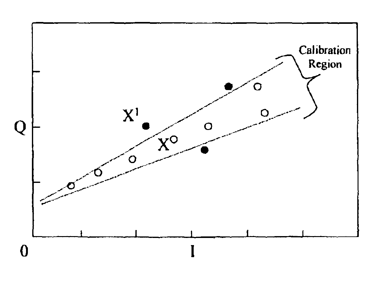
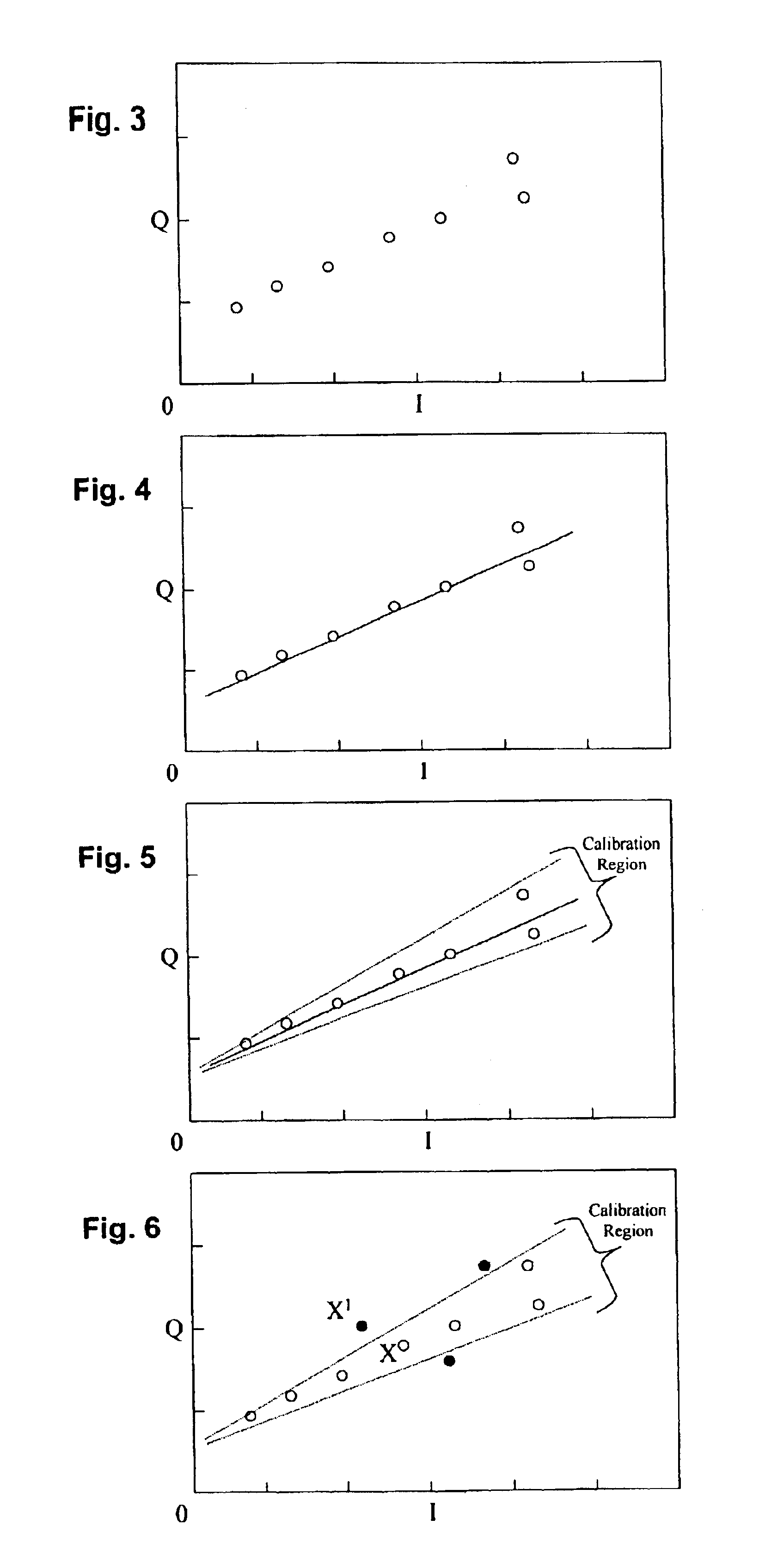
[0016]After creating the calibration region, the PMR-type optical system may be used to inspect and analyze semiconductor wafers. For each subject wafer, the PMR-type system makes one or more measurements. Measurements that fall within the calibration region are known to share the damage profile of the calibration subject. Measurements that do not fall within this region are assumed to deviate from the known damage profile of the calibration subject. This test provides an effective method of accepting or rejecting wafers that provide acceptable accuracy even when dopant concentrations are high or where heavy ions have been implanted.

Problems solved by technology

The ion implantation damages the crystal lattice as incoming ions come to rest.
This damage is typically proportional to the concentration and depth of ions within the crystal lattice.
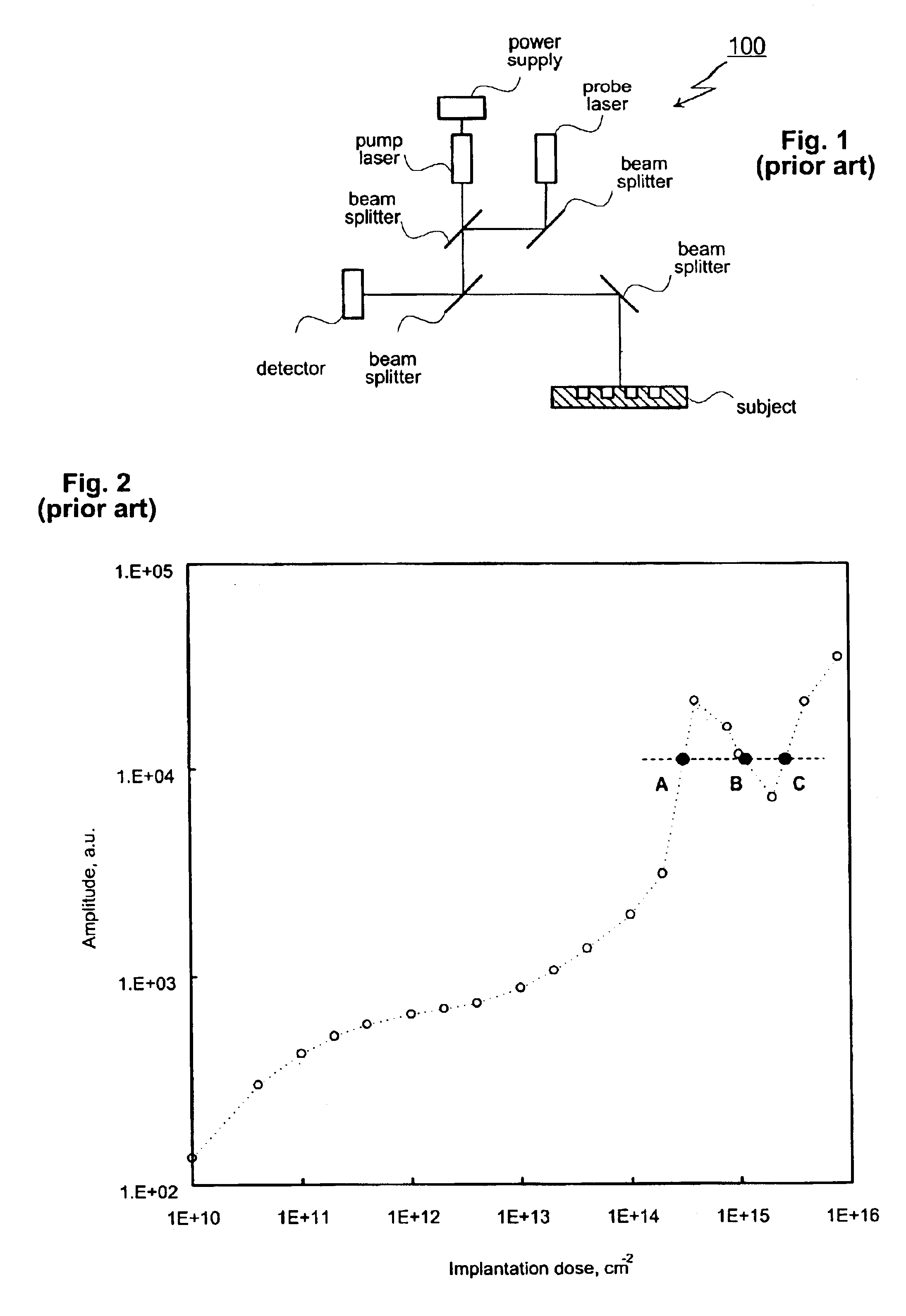
In fact, at high concentrations, the amplitude measurements are no longer well behaved and as a result cannot be used to accurately derive corresponding dopant concentrations.
In both cases, this is attributable to the appearance of a Si amorphous layer resulting in optical interference effects.

Method used


Image

  • Ion implant monitoring through measurement of modulated optical response
  • Ion implant monitoring through measurement of modulated optical response
  • Ion implant monitoring through measurement of modulated optical response

Examples


Embodiment Construction

[0025]The present invention provides a method for simultaneously measuring ion implantation dose, damage and / or dopant depth profiles in ion-implanted semiconductors. The measurement method is logically divided into two steps: a calibration and a measurement step. During the calibration step, the photo-modulated reflectance of a known damage profile is characterized. Typically, this involves identifying one or more areas within I-Q space that correspond to the photo-modulated reflectance of the known damage profile. All other areas within I-Q space are then assumed to be dissimilar to the known damage profile. In the measurement step, I-Q measurements for a test subject are obtained empirically. The empirically obtained I-Q measurements are then compared to determine if they fall within an identified region of I-Q space. This comparison indicates whether the test subject has a damage profile that is similar to the known damage profile. The following sections describe several possibl...


PUM


Abstract

A method for simultaneously monitoring ion implantation dose, damage and / or dopant depth profiles in ion-implanted semiconductors includes a calibration step where the photo-modulated reflectance of a known damage profile is identified in I-Q space. In a following measurement step, the photo-modulated reflectance of a subject is empirically measured to obtain in-phase and quadrature values. The in-phase and quadrature values are then compared, in I-Q space, to the known damage profile to characterize the damage profile of the subject.

Description

PRIORITY CLAIM[0001]This application claims priority from prior provisional application Ser. Nos. 60 / 365,237, filed Mar. 18, 2002, and 60 / 378,140, filed May 14, 2002, both of which are incorporated herein by reference.TECHNICAL FIELD[0002]The subject invention relates to optical devices used to non-destructively evaluate semiconductor wafers. In particular, the present invention relates to systems for measuring dopant concentrations in semiconductor samples.BACKGROUND OF THE INVENTION[0003]As geometries continue to shrink, manufacturers have increasingly turned to optical techniques to perform non-destructive inspection and analysis of semiconductor wafers. The basis for these techniques is the notion that a subject may be examined by analyzing the reflected energy that results when an optical beam is directed at a subject. This type of inspection and analysis is known as optical metrology and is performed using a range of different optical techniques.[0004]One widely used type of o...

Claims


Application Information

Patent Timeline
Patent Type & Authority Patents(United States)
IPC IPC(8): G01N21/00G01N21/55G01N21/27G01N21/35
CPCG01N21/276G01N21/55G01N2021/3568G01N21/1717
Inventor SALNIK, ALEXNICOLAIDES, LENAOPSAL, JON
Owner THERMA WAVE INC
Learn More