Supercharge Your Innovation With Domain-Expert AI Agents!

Method for error detection/correction of multilevel cell memory and multilevel cell memory having error detection/correction function

a multi-level cell memory and error detection technology, applied in the field of error detection/correction of multi-level cell memory and multi-level cell memory having error detection/correction function, can solve the problem that memory cells capable of storing two bits of information can lose control of threshold voltage in write operations, data error occurs in the memory, and the probability of two-bit errors in the same memory cell is higher

Inactive Publication Date: 2006-01-24
MONTEREY RES LLC
View PDF15 Cites 21 Cited by
  • Summary
  • Abstract
  • Description
  • Claims
  • Application Information

AI Technical Summary

Benefits of technology

[0019]An object of the present invention is to provide a multilevel cell memory capable of storing a plurality of bits of information in each single memory cell, in which reliable error detection / correction is performed by a simple method.
[0020]Another object of the present invention is to provide a multilevel cell memory capable of storing a plurality of bits of information in each single memory cell, in which error detection and error correction are achieved by a simple circuit without an increase in chip size.

Problems solved by technology

That is, a data error occurs in the memory cell having a physical bit address PA of “2”.
Four-level cell flash memories having memory cells capable of storing two bits of information can lose control of threshold voltages in write operations if defects occur among the memory cells.
This means higher chances of a two-bit error in the same memory cell.
Accordingly, multilevel cell flash memories of this type cannot fully relieve defects by simply performing the detection / correction of single-bit errors.
Nevertheless, conventional circuits for detecting / correcting two-bit errors are far more complicated than those for detecting / correcting single-bit errors.
Therefore, the implementation of a two-bit error detecting / correcting circuit on a flash memory has caused problems of greater chip sizes and increased fabrication costs.
Moreover, a two-bit error detecting / correcting circuits have longer error-detecting / correcting times as compared with single-bit error detecting / correcting circuits.
Furthermore, semiconductor memories that store eight levels and sixteen levels in each single memory cell are apt to three-bit errors and four-bit errors, respectively.
Nevertheless, there has been proposed no error-detection / correction technique that is tailored to a multi-bit defect occurring in a single multilevel memory cell.

Method used


Image

  • Method for error detection/correction of multilevel cell memory and multilevel cell memory having error detection/correction function
  • Method for error detection/correction of multilevel cell memory and multilevel cell memory having error detection/correction function
  • Method for error detection/correction of multilevel cell memory and multilevel cell memory having error detection/correction function

Examples


first embodiment

[0113]FIG. 8 shows the present invention. The multilevel cell memory is formed as a floating gate type four-level cell flash memory capable of storing two bits of information in each single memory cell. In this flash memory, the amounts of carriers to be trapped in the floating gates of memory cells are adjusted in four levels according to write data. Then, four types of memory cell currents corresponding to the threshold voltages of the memory cells are detected to read two bits of data stored in the memory cells.

[0114]The flash memory has a page buffer 10 and a memory core 12, as well as not-shown input circuits, output circuits, control circuits, and the like. The page buffer 10 has a buffer control circuit 14, data buffers 16 and 18, and an ECC control circuit 20. The memory core 12 includes a memory cell array 22 which is composed of a data area and a spare area, including a plurality of pages, and an operation control circuit 24 which performs read operations, write operations...

third embodiment

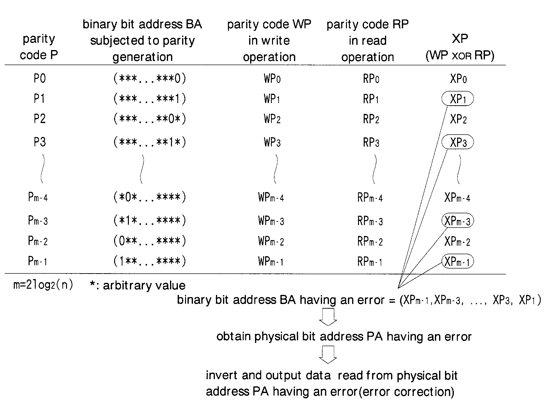
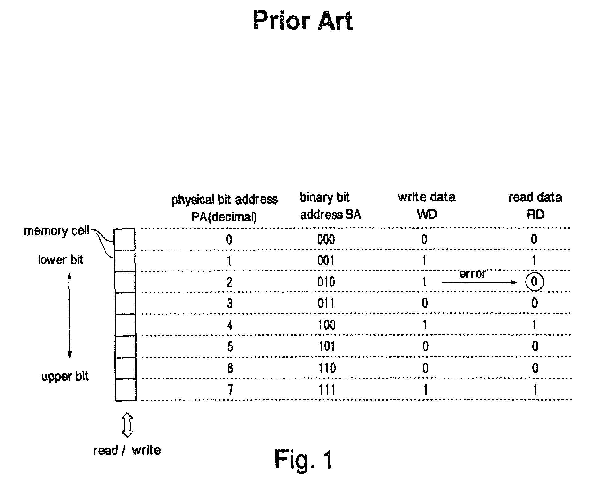
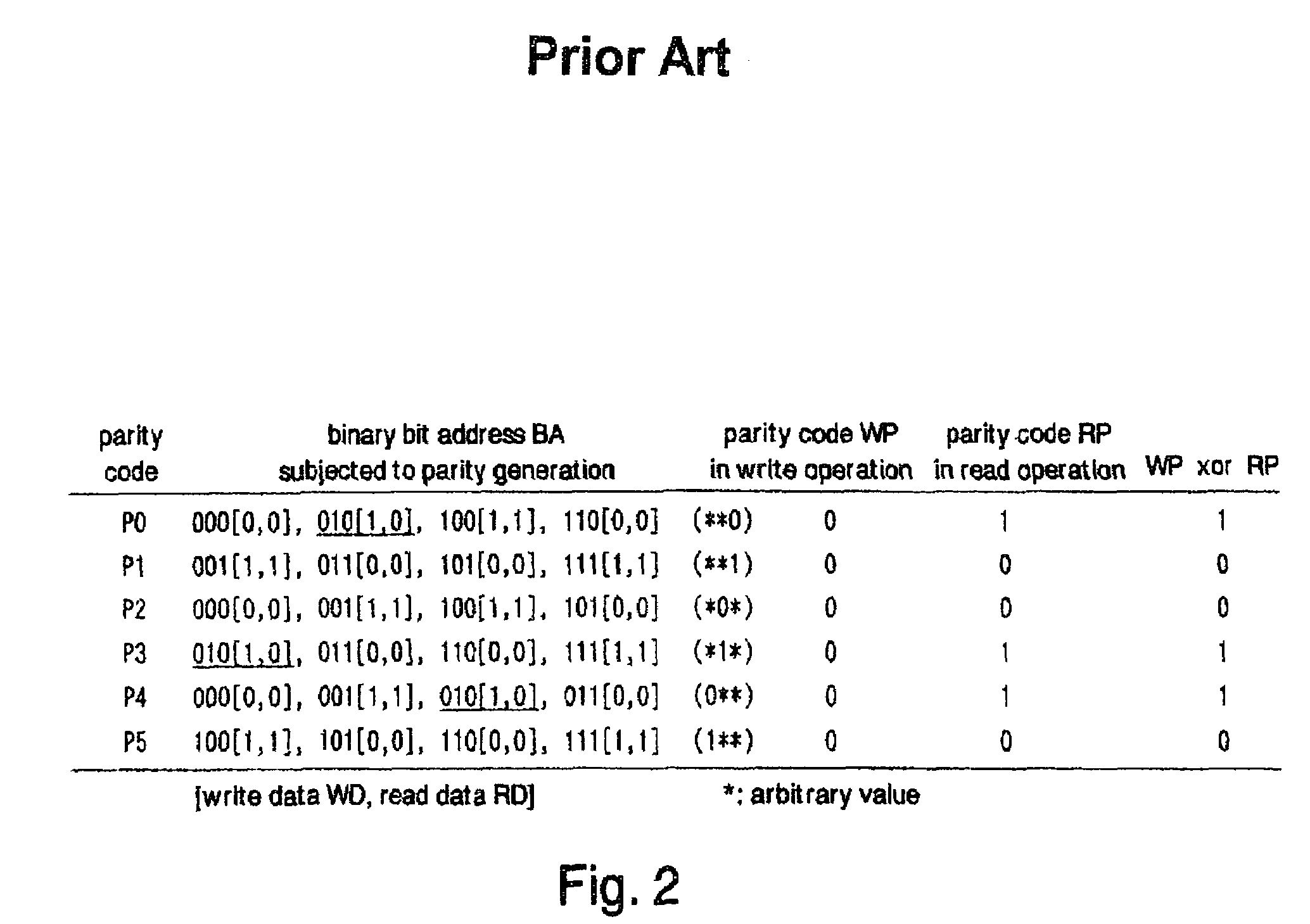
[0188]FIG. 27 shows memory cell addressing in the For ease of description, the number of memory cells to be accessed simultaneously in this example shall be four. That is, eight bits of data is read / written from / to memory cells by a single access. The individual bits of the memory cells are designated by physical addresses PA. The memory cells are designated by respective binary cell addresses BCA.

[0189]Since the memory cells store two bits each, there are provided a single first group A1 and a single second group Bi corresponding to this first group A1.

[0190]FIG. 28 shows the combinations of binary first addresses BA1 for generating the first parity codes PC1.

[0191]FIG. 29 shows the combinations of binary second addresses BA2 for generating the second parity codes PC2.

[0192]FIG. 30 shows the details of the first generating circuit 32a and the second generating circuits 32b shown in FIG. 26. The first generating circuit 32a generates the first parity codes PC1 shown in FIG. 28 (L0A...


PUM


Abstract

Binary bit addresses for error detection designating the individual bits of multilevel memory cells for retaining two bits of data, respectively, are assigned so that pairs of the binary bit addresses corresponding to each of the memory cells are mutually exclusive in each digit. For each digit of the binary bit addresses, first parity codes including a parity code of data corresponding to all the binary bit addresses having “0” in the digit and a parity code of data corresponding to all the binary bit addresses having “1” in the digit are generated for both write data and read data. The presence of a memory cell storing erroneous data in both bits is detected when all the first parity codes of the read data are different from the first parity codes of the write data. Thus, the multilevel cell memory can perform reliable error detection / correction by a simple method.

Description

CROSS REFERENCE TO RELATED APPLICATION[0001]This application is a continuation-in-part application of U.S. application Ser. No. 09 / 962,148, filed Sep. 26, 2001 now abandoned.BACKGROUND OF THE INVENTION[0002]1. Field of the Invention[0003]The invention relates to a method for error detection / correction of a multilevel cell memory which can store a plurality of bits of information in each single memory cell.[0004]2. Description of the Related Art[0005]In general, semiconductor memories store a single bit of information in each single memory cell thereof. In writing and reading data, such semiconductor memories as a flash memory generate simple error correcting codes (ECCs) by access to their memory cells, and compare these ECCs to perform the detection / correction of single-bit errors.[0006]FIGS. 1 and 2 show a method for detecting / correcting a single-bit error in a flash memory. For simplicity, the following description deals with the case of accessing (writing / reading) memory cells i...

Claims


Application Information

Patent Timeline
Patent Type & Authority Patents(United States)
IPC IPC(8): G11C29/00G06F11/10G11C11/56H03M13/11
CPCG06F11/1072H03M13/11G11C11/56
Inventor FURUKAWA, HIDEYUKI
Owner MONTEREY RES LLC
Features
  • R&D
  • Intellectual Property
  • Life Sciences
  • Materials
  • Tech Scout
  • Unparalleled Data Quality
  • Higher Quality Content
  • 60% Fewer Hallucinations
Learn More