Printed inductor capable of raising Q value
a technology of inductors and inductors, applied in the field of printed inductors, can solve the problems of increasing the ratio of conductor patterns occupying the insulating substrate, difficult to effectively form these inductors on the limited region of the insulating substrate, and difficulty in raising the q value of the resonance circuit, so as to reduce the degree of dielectric bonding and raise the q value
- Summary
- Abstract
- Description
- Claims
- Application Information
AI Technical Summary
Benefits of technology
Problems solved by technology
Method used
Image

Examples
first embodiment
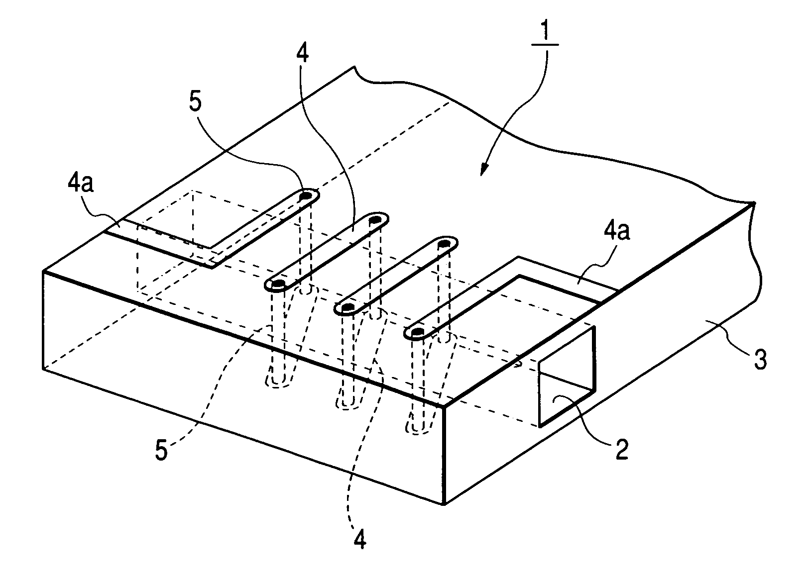
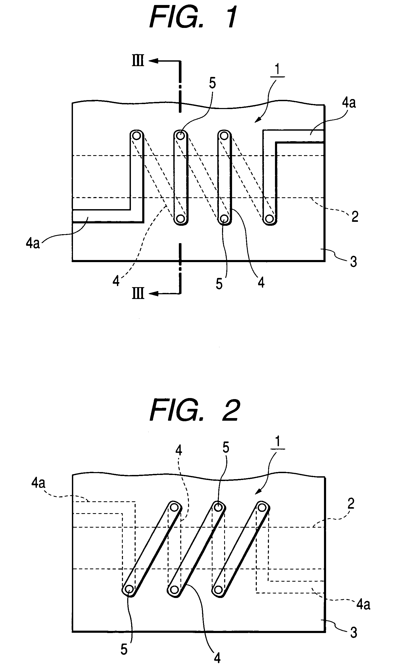
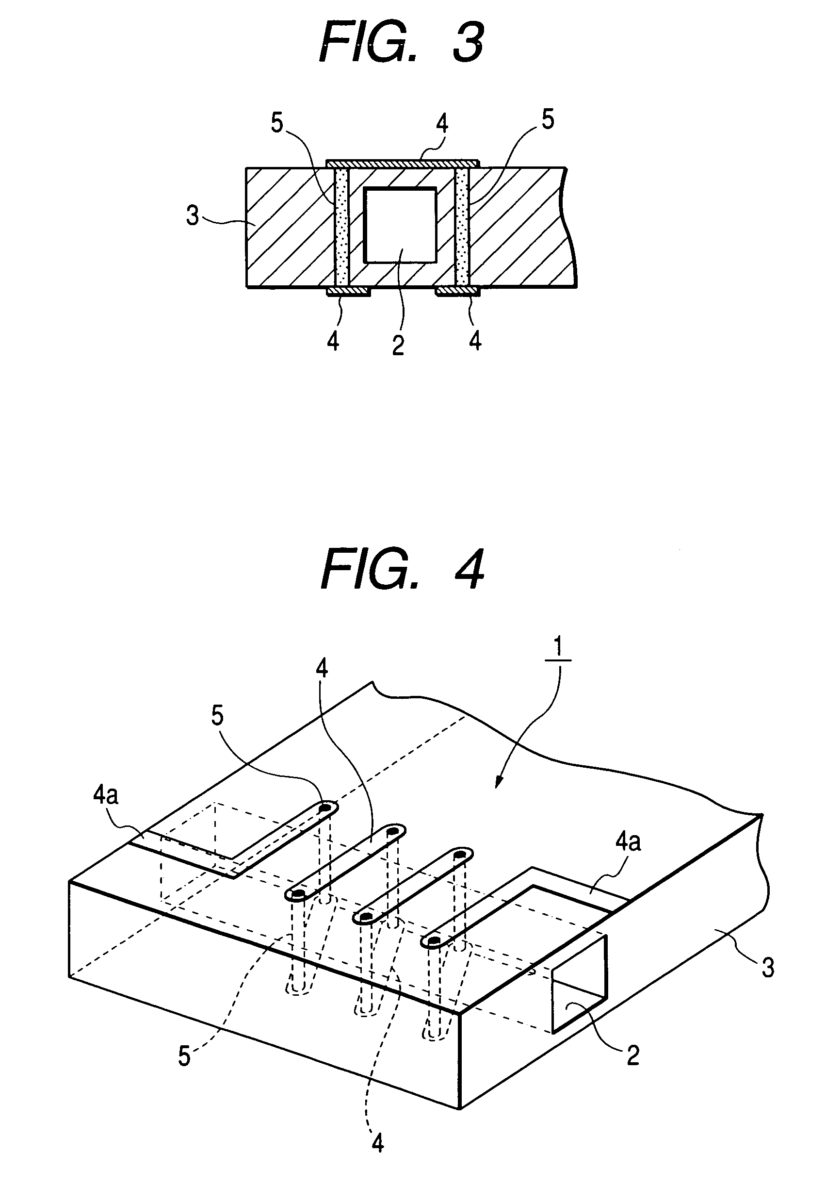
[0024]As shown in those drawings, the printed inductor 1 comprises an insulating substrate 3 having a cavity 2, a plurality of mutually independent printed wiring lines 4 formed on both the top and bottom faces of the insulating substrate 3, respectively, a plurality of through holes 5 for sequentially and continuously connecting terminals of the printed wiring lines 4 on the top and bottom faces to each other. The printed wiring lines 4 and the through hole 5 are formed in a spiral coil as the cavity 2 is regarded as the center of axis.
[0025]The insulating substrate 3 is made of, for example, a low temperature co-fired ceramic substrate, which is formed by mixing a crystallized glass with ceramic, and baking a green sheet obtained after kneading these materials at around 900° C. The cavity 2 extends in the insulating substrate 3 in a direction orthogonal to that of the thickness thereof. As apparent from FIG. 3, the cross-sectional shape of the cavity is a rectangular shape. The c...
second embodiment
[0029]FIG. 5 is a cross-sectional view of a printed inductor according to the present invention. In FIG. 5, similar reference numerals are given to elements corresponding to FIG. 1 to FIG. 4.
[0030]Except that the cavity 2 is filled with a magnetic material 6, the second embodiment is basically identical to the first embodiment in configuration. The magnetic material 6 is made of ferrite having a high magnetic permeability. The magnetic material 6 may be inserted into the cavity 2 from the end face thereof after baking the insulating substrate 3. Otherwise, the magnetic material 6 may be buried in the cavity 2 after being buried in the green sheet.
[0031]According to the printed inductor of the second embodiment constructed as described above, the magnetic material 6 can fill the cavity 2 using a broad space therein. As a result, the second embodiment has the same effect as that of the first embodiment. In addition, it is possible to raise an inductance value largely. Further, by sele...
third embodiment
[0032]FIG. 6 is a cross-sectional view of a printed inductor according to the present invention. Similar reference numerals are given to elements corresponding to FIG. 1 to FIG. 4.
[0033]Except that the low temperature co-fired ceramic substrate 7 is used as the insulating substrate, and a magnetic material 9 made of ferrite, etc., is attached to the inner wall surface of the cavity 8, which is provided in the low temperature co-fired ceramic substrate (LTCC) 7, the third embodiment is basically identical to the first embodiment in configuration. The low temperature co-fired ceramic substrate 7 is obtained by superposing at least two or more low temperature co-fired ceramics 7A, 7B as much as the necessary number of sheets. Concave portions 8a, 8b of these low temperature co-fired ceramics 7A, 7B is caused to face each other, thereby forming the cavity 8 having a section of a rectangular shape. The magnetic material 9 is formed by baking magnetic paste, which is mixed with magnetic p...
PUM
 Abstract
Description
Claims
Application Information
 - R&D
- Intellectual Property
- Life Sciences
- Materials
- Tech Scout
- Unparalleled Data Quality
- Higher Quality Content
- 60% Fewer Hallucinations
Browse by: Latest US Patents, China's latest patents, Technical Efficacy Thesaurus, Application Domain, Technology Topic, Popular Technical Reports.
© 2025 PatSnap. All rights reserved.Legal|Privacy policy|Modern Slavery Act Transparency Statement|Sitemap|About US| Contact US: help@patsnap.com