Semiconductor device

a technology of semiconductors and devices, applied in the direction of solid-state devices, basic electric elements, electrical apparatus construction details, etc., to achieve the effect of simplifying circuit patterns, reducing the adverse effect of wiring inductance, and facilitating injection

Inactive Publication Date: 2006-02-07
FUJI ELECTRIC CO LTD
View PDF7 Cites 51 Cited by
  • Summary
  • Abstract
  • Description
  • Claims
  • Application Information

AI Technical Summary

Benefits of technology

[0016]According to the above described assembled structure of the semiconductor device, the power circuit, enclosure case, control terminal block, control circuit, and case top cover can be stacked together from above to be assembled. This structure easily accommodates an automatic assembly method using an assembly robot. Further, a distance of wiring path can be minimized to connect between the main circuit terminals and power circuit, the power circuit and control circuit, and the control circuit and control terminals, thereby preventing malfunction due to an adverse effect of wiring inductance. Furthermore, the gel-like filler can be quickly injected into the package so as to spread over the whole interior thereof.
[0029]Further, the main terminals may be lead terminals made of copper and are plated with nickel, solder, or gold to improve soldering characteristic of the copper lead terminals, bonding characteristic of the wires, and contact characteristic of the connectors.

Problems solved by technology

Moreover, when an intermediate inspection during an assembly process indicates that any of the components such as ICs mounted on the control circuit is defective, the defective control circuit can easily be replaced with a good one by removing a solder junction between the printed circuit board of the control circuit and the terminal leads.

Method used


Image

  • Semiconductor device
  • Semiconductor device
  • Semiconductor device

Examples


Embodiment Construction

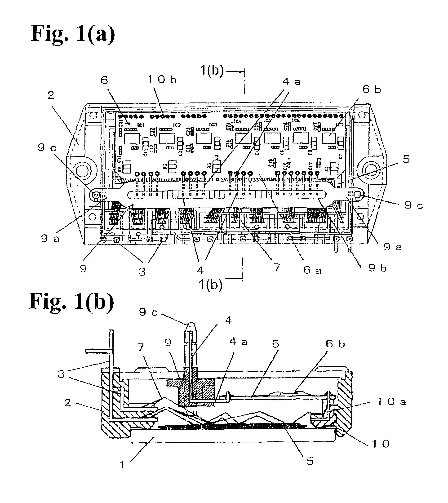
[0044]Hereunder, embodiments of the present invention will be described with reference to the accompanied drawings, using a power module applied to an inverter (three-phase) apparatus as an example.

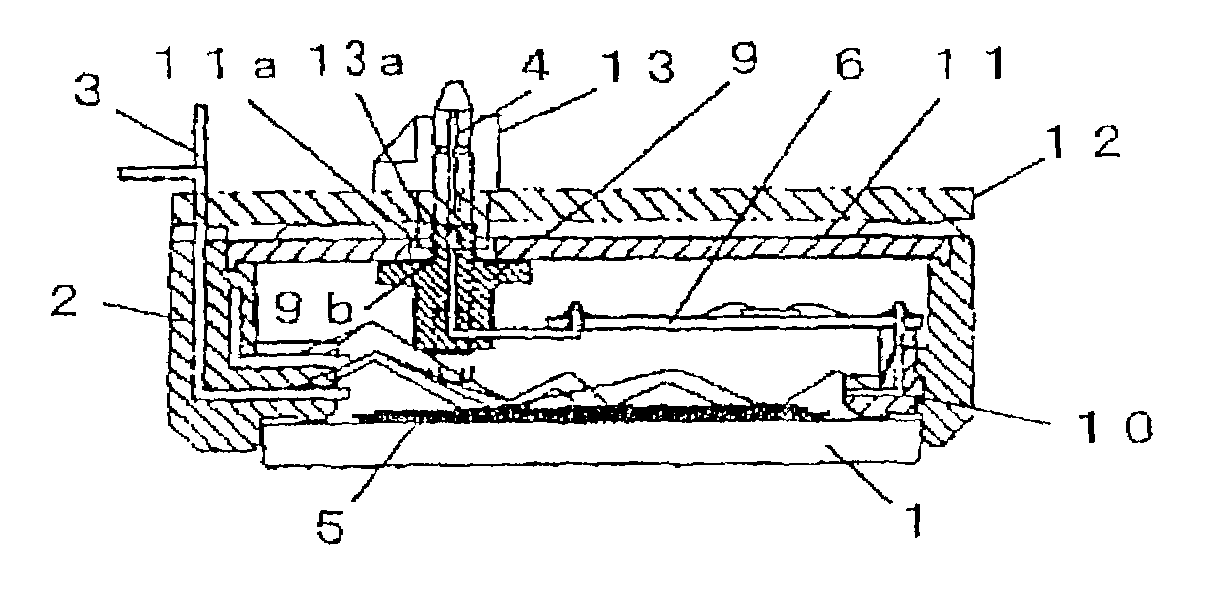
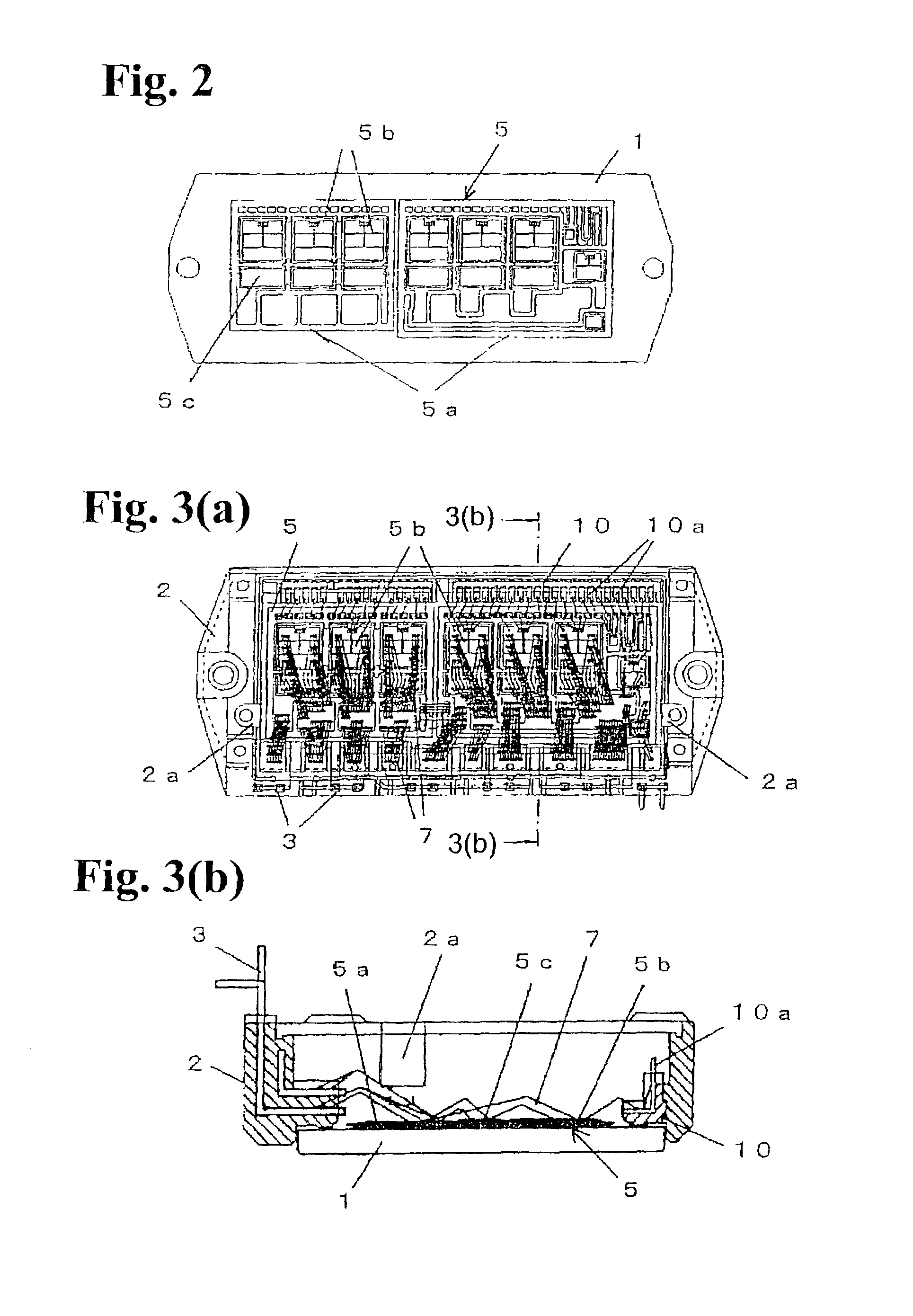
[0045]In the embodiments, members corresponding to FIGS. 12(a)–13(b) are denoted by the same reference numerals, thus description thereof is omitted. Further, in the figures of the embodiments, reference numeral 9 denotes a control terminal block assembled on a top surface side of an enclosure case 2 as an independent component; reference numeral 10 denotes a relay terminal block disposed along an inner peripheral side edge of the enclosure case 2; and reference numeral 11 denotes a case top cover placed on the top surface of the enclosure case 2. Furthermore, among terminal symbols marked on the case top cover in FIG. 4(a), reference characters P and N denote DC input terminals; reference characters U, V, and W denote AC output terminals for the respective phases; and reference numeral B...


PUM


Abstract

A semiconductor device includes a package composed of a metal base, an enclosure case integrated with terminals, and a top cover. A power circuit and a control circuit are arranged inside the package vertically, and a gel-like filler is injected to seal the package after being assembled. In this semiconductor device, externally lead control terminals for the control circuit are insert-molded in a control terminal block constituting an independent component. The control terminal block is fixed to the enclosure case to extend over a center of a top surface thereof. A printed circuit board of the control circuit is disposed and connected between the control terminal block and a relay terminal block disposed inside the case.

Description

BACKGROUND OF THE INVENTION AND RELATED ART STATEMENT[0001]The present invention relates to a semiconductor device applied to an intelligent power module for an inverter apparatus, and more specifically, relates to an assembled structure.[0002]First, an intelligent power module applied to an inverter apparatus will be described as an example of a conventional intelligent power module. An assembled structure of the example is shown in FIGS. 12(a) to 13(b).[0003]In the figures, reference numeral 1 denotes a radiating metal base (a copper base), reference numeral 2 denotes an enclosure case composed of a molded resin integrated with terminals, and reference numeral 3 denotes main terminals (external lead terminals, or screw terminals, for input and output of a power circuit and for a brake circuit). Reference numeral 4 denotes control terminals (external lead terminals, or pin terminals, used to input and output control signals to and from a control circuit), reference numerals 5 and 6...

Claims


Application Information

Patent Timeline
Patent Type & Authority Patents(United States)
IPC IPC(8): H01L23/02H01L23/22H01L23/24H01L23/28H05K7/20H01L23/045H05K1/14
CPCH01L23/045H01L23/24H01L2224/48137H01L2224/48247H01L2924/01078H01L2924/01068H01L2924/13055H01L2924/30107H05K1/144H01L24/48H01L2924/01079H01L2224/48095H01L2224/49111H01L2224/85444H01L2224/85455H01L2224/45099H01L2924/00014H01L2924/181H01L24/49H01L2924/00H01L2224/45015H01L2924/207
Inventor SOYANO, SHINMOCHIZUKI, EIJI
Owner FUJI ELECTRIC CO LTD
Why Eureka
Try Eureka