Display device with an array of display drivers recessed onto a substrate

a display device and substrate technology, applied in the direction of static indicating devices, semiconductor/solid-state device details, instruments, etc., can solve the problems of feds, reducing productivity, and being typically manufactured in a batch operation

Inactive Publication Date: 2006-02-14
RUIZHANG TECH LTD CO
View PDF8 Cites 63 Cited by
  • Summary
  • Abstract
  • Description
  • Claims
  • Application Information

AI Technical Summary

Problems solved by technology

There are several disadvantages inherent to display devices such as FEDs.
This is inefficient because a portion of the emitters will be inoperable.
This reduces productivity because it is more efficient to use a method in which premanufactured objects are quickly placed onto a layer.
Another disadvantage to existing FEDs is that they are typically manufactured in a batch operation.
Batch operations inherently involve a certain amount of down-time in production.
This increases aggregate production time to fabricate display panels.
This also decreases productivity since the assembly of the flat-panel displays is interrupted until another panel is available to assemble the flat-panel display.
There are also several disadvantages associated with conventional plasma displays.
This reduces productivity because it is more efficient to use a method in which objects are quickly placed onto the rigid substrate, such as through fluidic self assembly.
Another disadvantage to plasma displays is that they are also typically manufactured in a batch operation.

Method used


Image

  • Display device with an array of display drivers recessed onto a substrate
  • Display device with an array of display drivers recessed onto a substrate
  • Display device with an array of display drivers recessed onto a substrate

Examples


Embodiment Construction

[0077]The present invention relates to apparatuses and methods for forming displays and other electronic assemblies. The following description and drawings are illustrative of the invention and are not to be construed as limiting the invention.

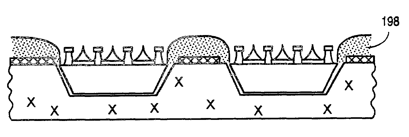
[0078]One embodiment of the invention relates to using FSA to form a display such as a FED display. Incorporated by reference is U.S. Pat. No. 5,545,291 explaining how to assemble objects onto a substrate using FSA. The FSA with a plurality of objects is deposited onto the substrate wherein the objects fall into recessed regions found in the substrate. One embodiment has the objects (e.g., blocks having emitters and gates, spacers, and driver chips) being transferred at one time.

[0079]The various objects may be placed into recessed regions of a substrate by using FSA first for the largest objects. After the largest objects are placed in the largest recessed regions of the substrate using a first slurry, a second slurry containing the next smal...


PUM


Abstract

Apparatuses and methods for forming displays are claimed. One embodiment of the invention relates to dispensing display drivers over a substrate. The display drivers, for example, may be a plurality of emitters and gates in order to form a display such as a field emission display (FED). Alternatively, the display drivers may be rods for a plasma display. Another embodiment of the invention relates to forming an electronic device along a length of substrate using template transfer or FSA to deposit display drivers into recessed regions or holes of a substrate. Another embodiment of the invention relates to using FSA and a deterministic method such as “pick and place” to place display drivers onto a substrate. Another embodiment of the invention relates to using donor transfer of display drivers to a substrate.

Description

BACKGROUND INFORMATION[0001]1. Field of the Invention[0002]The present invention relates generally to the manufacturing of electronic assemblies, and more particularly to the manufacture of display devices.[0003]2. Description of Related Art[0004]Electronic assemblies such as display devices are known in the art. Display devices include a variety of displays such as field emission displays (FEDs), plasma display devices, and other suitable display devices. Each of these display devices are described below.[0005]FEDs are generally used for television images, oscilloscope radar displays, computer displays, and other like applications. FIG. 1 illustrates a cross-sectional view of a FED known in the art. FEDs are comprised of anode 2 and cathode 8. Anode 2 comprises multiple layers of material. These multiple layers include a face layer 6, a vacuum layer 18, a conductive layer 20, and a luminescent layer 22. As noted in U.S. Pat. No. 5,818,165, the face layer 6 of the anode 2 may be com...

Claims


Application Information

Patent Timeline
Patent Type & Authority Patents(United States)
IPC IPC(8): H01L29/06
CPCH01J5/54H01L24/95H01L29/06H01J2217/49H01L2924/1306H01L2924/01041H01L2924/01033H01J2329/92H01L2224/95085H01L2924/01002H01L2924/01004H01L2924/0101H01L2924/01013H01L2924/01015H01L2924/01018H01L2924/01027H01L2924/01029H01L2924/0104H01L2924/01042H01L2924/01049H01L2924/01054H01L2924/01074H01L2924/01079H01L2924/15155H01L2924/15165H01L2924/19041H01L2924/19043H01L2924/01005H01L2924/01023H01L2924/15153H01L2924/00
Inventor BOLING, EDWARDJACOBSEN, JEFFREY JAYNOWICKI, RONALD STEPHEN
Owner RUIZHANG TECH LTD CO
Why Eureka
Try Eureka