Image sensor and method of fabricating the same

a technology of image sensor and manufacturing method, which is applied in the field of semiconductor devices, can solve the problems of increasing the occurrence of dark defects, difficult high integration and high power dissipation, etc., and achieve the effect of reducing dark defects

Inactive Publication Date: 2006-02-28
SAMSUNG ELECTRONICS CO LTD
View PDF4 Cites 34 Cited by
  • Summary
  • Abstract
  • Description
  • Claims
  • Application Information

AI Technical Summary

Benefits of technology

[0016]It is a feature of the present invention to provide an image sensor to reduce dark defects and a method of fabricating the same.
[0017]It is another feature of the present invention to provide an image sensor to improve color distinction of a picture and a method of fabricating the same.

Problems solved by technology

The CCD image sensor has sensitivity and noise characteristics that are superior to the CMOS image sensor, but has disadvantages which include difficulty of high integration and high power dissipation.
The dark current may increase the occurrence of dark defects that result when pixels operate without light.

Method used


Image

  • Image sensor and method of fabricating the same
  • Image sensor and method of fabricating the same
  • Image sensor and method of fabricating the same

Examples


Embodiment Construction

[0033]Preferred embodiments of the present invention will be described below in more detail with reference to the accompanying drawings. This invention may, however, be embodied in different forms and should not be constructed as limited to the embodiments set forth herein. Rather, these embodiments are provided so that this disclosure will be thorough and complete, and will fully convey the scope of the invention to those skilled in the art. In the drawings, the thickness of layers and regions are exaggerated for clarity. It will also be understood that when a layer is referred to as being “on” another layer or substrate, it can be directly on the other layer or substrate or intervening layers may also be present. Like numbers refer to like elements throughout the specification.

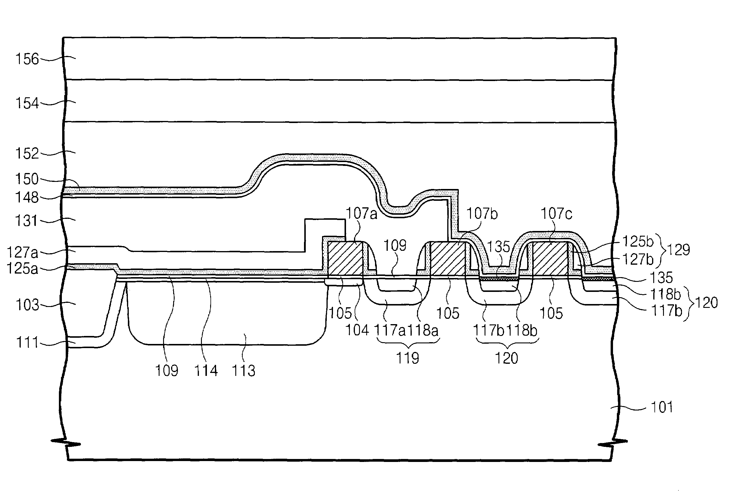
[0034]FIG. 3 is a top plane view of an image sensor in accordance with a preferred embodiment of the present invention. FIG. 4 is a cross-sectional view of the image sensor taken along a line I–I′ of FIG. 3....


PUM


Abstract

Image sensors and methods of fabricating the same are provided. The image sensor includes a blocking pattern disposed on photodiodes. The blocking pattern is formed of insulation material having a metal diffusion coefficient which is lower than a silicon oxide diffusion coefficient. Therefore, dark defects of the image sensor are reduced. In addition, the image sensor includes a color-ratio control layer. The color ratio control layer controls color ratios between the sensitivities to blue, green and red. As a result, color distinction of the picture that is embodied by the image sensor can be improved.

Description

FIELD OF THE INVENTION[0001]The present invention relates to a semiconductor device and a method of fabricating the same and more specifically to a CMOS image sensor and a method of fabricating the same.BACKGROUND OF THE INVENTION[0002]Image sensors play a role in transforming optical images to electrical signals. The image sensors are classified into two major categories, including a complementary metal-oxide-silicon (CMOS) image sensor and a charge coupled device (CCD) image sensor. The CCD image sensor has sensitivity and noise characteristics that are superior to the CMOS image sensor, but has disadvantages which include difficulty of high integration and high power dissipation. The CMOS image sensor has advantages which include simple fabrication, suitability for high integration and low power dissipation.[0003]Recently, there have been improvements in fabrication of CMOS devices and the characteristics thereof. Moreover, extensive studies on the CMOS image sensor have been per...

Claims


Application Information

Patent Timeline
Patent Type & Authority Patents(United States)
IPC IPC(8): H01L27/108H01L27/00H01LH01L27/146H01L27/14H01L31/00
CPCH01L27/14603H01L27/14609H01L27/1462H01L27/14689H01L27/14685H01L27/14621H01L27/14645
Inventor SONG, JAE-HOPARK, YOUNG-HOONSHIN, SANG-HAK
Owner SAMSUNG ELECTRONICS CO LTD
Why Eureka
Try Eureka