Three-terminal magnetostatically coupled spin transfer-based MRAM cell

a spin transfer and mram cell technology, applied in the field of three-terminal magnetostatically coupled spin transfer-based mram cells, can solve the problem of not being able to reduce the high operating current sufficiently

Active Publication Date: 2006-03-07
SAMSUNG SEMICON
View PDF6 Cites 405 Cited by
  • Summary
  • Abstract
  • Description
  • Claims
  • Application Information

AI Technical Summary

Problems solved by technology

However, using such a spin transfer system presents two primary challenges.
Ho...

Method used


Image

  • Three-terminal magnetostatically coupled spin transfer-based MRAM cell
  • Three-terminal magnetostatically coupled spin transfer-based MRAM cell
  • Three-terminal magnetostatically coupled spin transfer-based MRAM cell

Examples


second embodiment

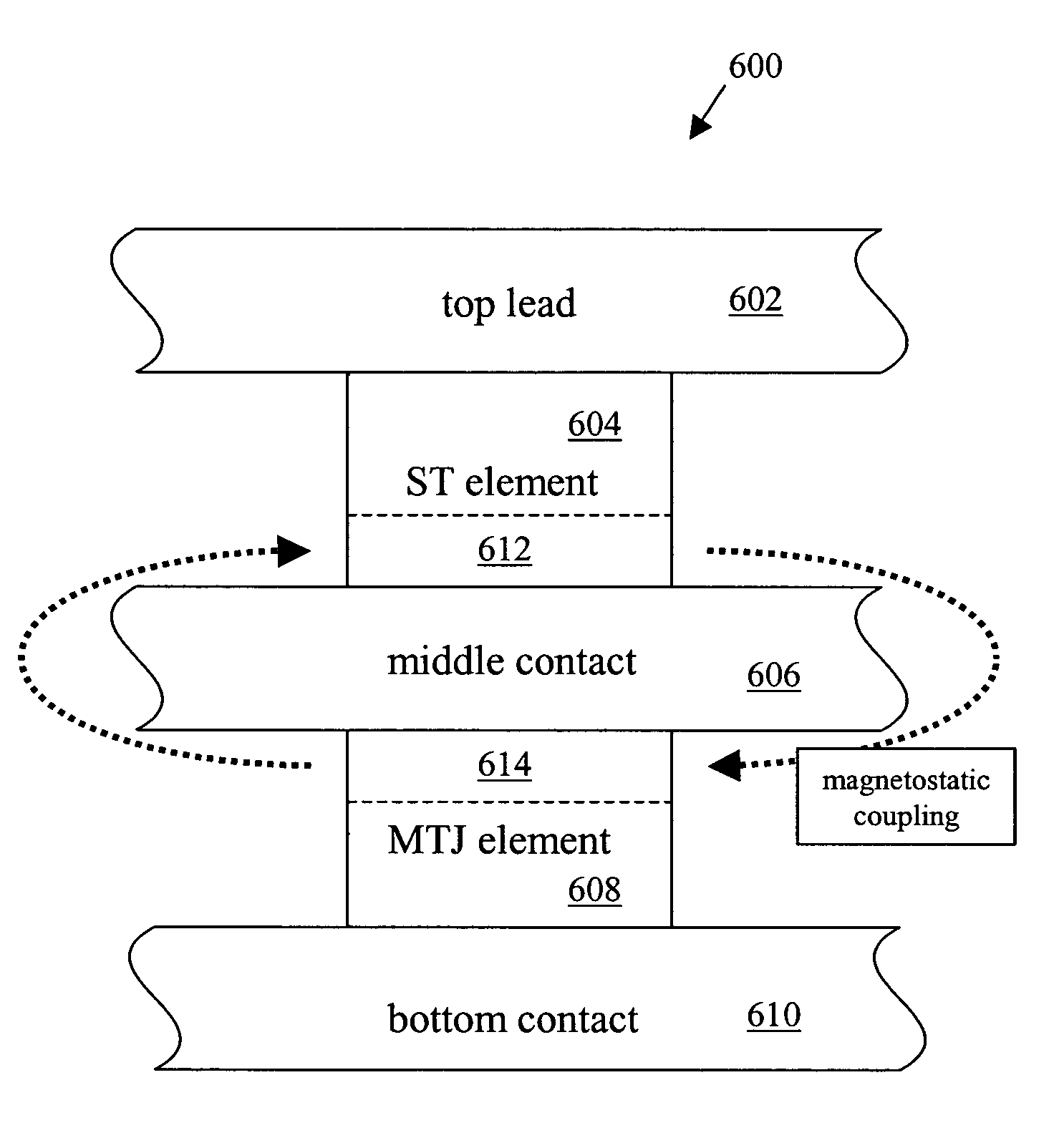
[0057]FIG. 14 illustrates the second embodiment in a structural layout with like numbers designating the like elements in FIG. 13. Thus, a write operation includes sending a current pulse through the bridging contact 1309, through a middle contact 1306, and then through the spin transfer element 1304. This can be achieved by applying a voltage along WL 1310 as well as a voltage on BL 1302, while grounding GL 1312 and the shared transistor source 1314.

[0058]A read operation includes sending a current pulse through the MTJ element 1308 and then through the spin transfer element 1304. This can be achieved by applying a voltage along WL 316 as well as a voltage on the BL 1302, while grounding GL 1312. As the read current flows through both the MTJ readout element 1308 and the spin transfer element 1304, the resistance of the MTJ readout element 1308 must be carefully chosen such that the read current does not also write the device 1300.

third embodiment

[0059]A third embodiment, illustrated in FIG. 15, uses two transistors 1520, 1522 per cell 1500 for isolation and selection. However, the middle contact line 1505 is used as the bit line BL 1506. In this configuration, the write current can be directed solely through the spin transfer element 1504, and the read current can be directed solely through the MTJ readout element 1508. Thus, the resistance of the MTJ element 1508 does not need to be tailored such that the read current is limited to be smaller than the write current.

[0060]A write operation includes sending a current pulse through the bit line 1506, through the transistor 1520 connected directly to the spin transfer element 1504, through the spin transfer element 1504, and then out to the ground line GL 1506. This can be achieved by applying a voltage along the gate WL 1510 of the transistor 1520 as well as a voltage on BL 1506, while grounding GL 1512. A read operation includes sending a current pulse through the MTJ elemen...


PUM


Abstract

A magnetic memory device for reading and writing a data state comprises at least three terminals including first, second, and third terminals. The magnetic memory device also includes a spin transfer (ST) driven element, disposed between the first terminal and the second terminal, and a readout element, disposed between the second terminal and the third terminal. The ST driven element includes a first free layer, and a readout element includes a second free layer. A magnetization direction of the second free layer in the readout element indicates a data state. A magnetization reversal of the first free layer within the ST driven element magnetostatically causes a magnetization reversal of the second free layer in the readout element, thereby recording the data state.

Description

BACKGROUND[0001]1. Field[0002]The present invention relates generally to magnetic memory systems and, more particularly, to a method and system for providing an element that employs a spin-transfer effect in switching and that can be used in a magnetic memory, such as a magnetic random access memory (“MRAM”).[0003]2. Description of the Related Art[0004]Magnetic memories are often used for storing data. One type of memory element currently of interest utilizes magneto-resistance of a magnetic element for storing and reading data. FIGS. 1 and 2 depict conventional magnetic elements 100 and 200.[0005]The conventional magnetic element 100, shown in FIG. 1, is a spin valve (SV) 100 and includes a conventional anti-ferromagnetic (AFM) layer 110, a conventional pinned layer 108, a conventional spacer layer 106, which is typically a conductor, and a conventional free layer 104. The conventional pinned layer 108 and the conventional free layer 104 are ferromagnetic. The conventional spacer l...

Claims


Application Information

Patent Timeline
IPC IPC(8): G11C11/14
CPCG11C11/16H01L27/228H01L43/08H10B61/22H10N50/10
Inventor HUAI, YIMINGNGUYEN, PAUL P.ALBERT, FRANK
Owner SAMSUNG SEMICON
Why Eureka
Try Eureka