High data rate differential signal line design for uniform characteristic impedance for high performance integrated circuit packages

a technology of integrated circuit and characteristic impedance, which is applied in the direction of printed circuit non-printed electric components, semiconductor/solid-state device details, instruments, etc., can solve the problems of reducing signal quality and producing unwanted reflections, and achieve the effect of convenient signal line design, characteristic impedance, and increasing trace width and line spacing

Active Publication Date: 2006-03-14
AVAGO TECH INT SALES PTE LTD
View PDF10 Cites 6 Cited by
  • Summary
  • Abstract
  • Description
  • Claims
  • Application Information

AI Technical Summary

Benefits of technology

[0009]The present invention facilitates the design of signal lines suitable for transmitting high data-rate differential signal without inducing significant impacts to signal integrity. Signal lines that carry high data-rate differential signals are designed in a differential ended configuration. The characteristics impedance of the differential line pair, that transmits the signals, primarily depends on the line trace width, line spacing, and dielectric thickness. By properly varying the trace width and the spacing, the characteristic impedance will also vary.
[0010]In the present invention, the escape area of the differential signal line is designed to be, for example, about 100 ohms with a narrow trace width and narrow spacing between the signal lines. Particularly, the spacing between inverting and non-inverting paths of the differential signal line is selected such that the cross-talk is reduced to about 1% (−40 db). Beyond the escape area, the characteristic impedance can be maintained at about 100 ohms by increasing the trace width and line spacing. An advantage of increasing the trace width beyond the escape area is that the resistance of the line is reduced, ultimately reducing the insertion loss.

Problems solved by technology

For high pin-count packages, a significant challenge lies in escaping high data rate input / output (IO) differential signals from the IC, or die, to the package.
Unfortunately, however, these factors degrade signal quality by producing unwanted reflections due to the impedance mismatches, and signal coupling between the adjacent lines.

Method used


Image

  • High data rate differential signal line design for uniform characteristic impedance for high performance integrated circuit packages
  • High data rate differential signal line design for uniform characteristic impedance for high performance integrated circuit packages
  • High data rate differential signal line design for uniform characteristic impedance for high performance integrated circuit packages

Examples


Embodiment Construction

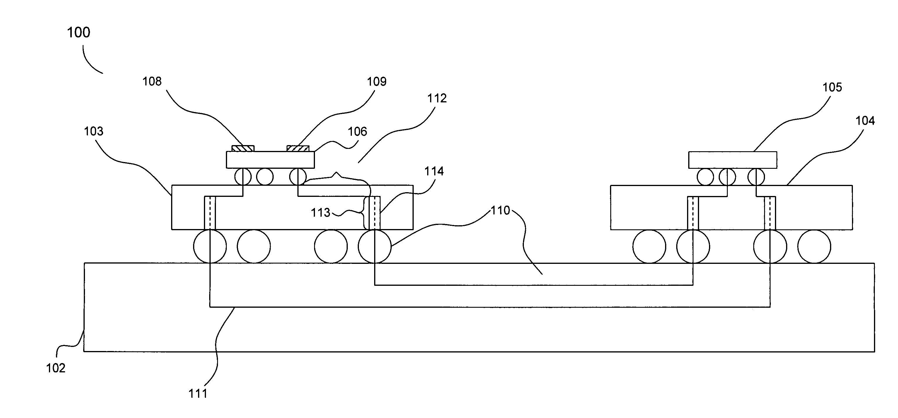
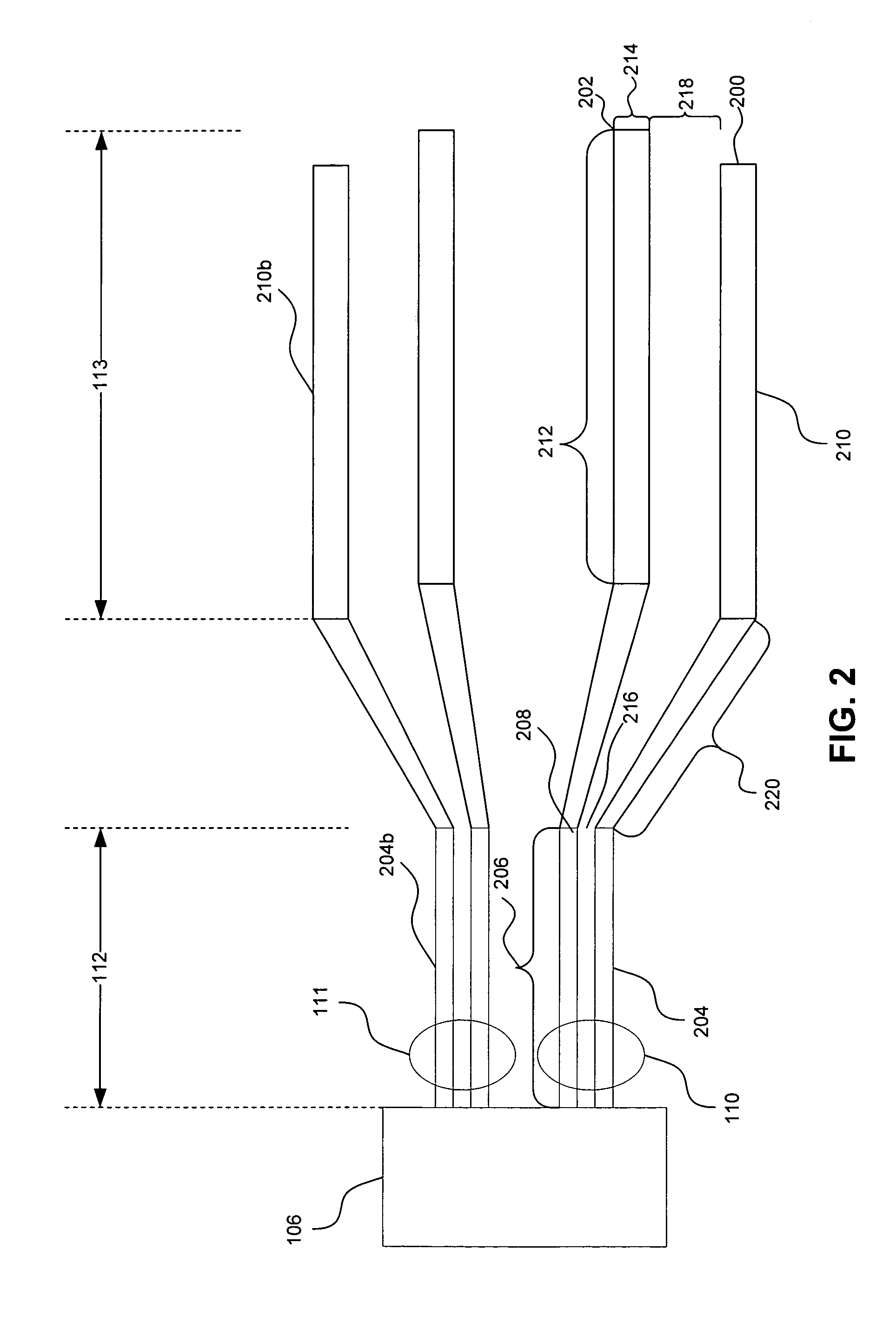
[0016]The following detailed description of the present invention refers to the accompanying drawings that illustrate exemplary embodiments consistent with this invention. Other embodiments are possible, and modifications may be made to the embodiments within the spirit and scope of the invention. Therefore, the detailed description is not meant to limit the invention. Rather, the scope of the invention is defined by the appended claims.

[0017]It would be apparent to one of skill in the art that the present invention, as described below, may be implemented in many different embodiments of software, hardware, firmware, and / or the entities illustrated in the figures. Any actual software code with the specialized control of hardware to implement the present invention is not limiting of the present invention. Thus, the operational behavior of the present invention will be described with the understanding that modifications and variations of the embodiments are possible, given the level o...


PUM


Abstract

Provided is an apparatus that includes an integrated circuit (IC) mounted on a chip carrier. The IC has one or more differential pair circuits coupled thereto and the chip carrier has a signal escaping portion and a remaining portion. The apparatus also includes differential signal lines coupled to the differential pair circuits, the differential signal lines (i) extending through the chip carrier and (ii) having first and second segments. The first segment extends through the escaping portion and the second segment extends through the remaining portion. The first and second segments have respective first and second widths.

Description

BACKGROUND OF THE INVENTION[0001]1. Field of the Invention[0002]The present invention relates generally to the field of integrated circuit (IC) design. In particular, the present invention relates to differential signal line design for multi giga-hertz GHz data rates on the high performance IC packages.[0003]2. Related Art[0004]For high pin-count packages, a significant challenge lies in escaping high data rate input / output (IO) differential signals from the IC, or die, to the package. In escaping these high data rate signals, a designer will preferably provide for escaping the signals without impacting signal integrity.[0005]Using conventional techniques, signals are escaped from the die near the die-package interface with virtually no concern for signal integrity. This approach might be suitable for relatively low frequency signals, i.e., signals having data rates below one giga-bit per second (Gbps). But as the signal data rates increase, for example, beyond about 5 Gbps, the met...

Claims


Application Information

Patent Timeline
Patent Type & Authority Patents(United States)
IPC IPC(8): G06F17/50H01L23/498H01L23/66H01P5/02H05K1/02H05K1/18
CPCH01L23/49838H01P5/02H05K1/025H01L23/66H01L2224/16225H01L2223/6627H01L2224/16H01L2924/15173H01L2924/15174H01L2924/15311H01L2924/1903H01L2924/3011H05K1/181H05K2201/09236H05K2201/09727H05K2201/10674H05K2201/10734H01L2924/00014H01L2224/0401
Inventor AGRAWAL, AMIT P.
Owner AVAGO TECH INT SALES PTE LTD
Why Eureka
Try Eureka