Stress-relieved shallow trench isolation (STI) structure and method for forming the same

a shallow trench isolation and stress-relief technology, applied in the direction of basic electric elements, semiconductor/solid-state device manufacturing, electric apparatus, etc., can solve the problems of forming defects in silicon substrates, forming defects in particular, and retaining stress between trench dielectric layers and surrounding semiconductor substrates during thermal cycling, so as to achieve the effect of substantially reducing the stress between the trench dielectric layer and the surrounding semiconductor substra

Inactive Publication Date: 2006-03-21
INTEGRATED DEVICE TECH INC
View PDF11 Cites 77 Cited by
  • Summary
  • Abstract
  • Description
  • Claims
  • Application Information

AI Technical Summary

Benefits of technology

[0014]With the present invention, the stress between the trench dielectric layer and the surrounding semiconductor substrate during thermal cycling can be substantially reduced by allowing the trench dielectric layer to be expanded or shrunk with the surrounding substrate without generating stress. This is believed to be possible because the buried void acts as a buffer structure during thermal cycling.

Problems solved by technology

However, conventional STI processes still have drawbacks.
For example, defects can be formed in the silicon substrate due to the thermo-mechanical stress placed on the silicon substrate and the dielectric material during the STI process.
The defects can be formed especially during the subsequent processes involving thermal cycles, such as various thermal oxidation, and source / drain implantation activation anneal processes.
That is, the trench sidewalls can be subjected to oxidation, increasing the trench dielectric volume, which in turn, builds up the stress.
The HDP oxide layer is very dense and is very susceptible to any thermal cycles applied on the STI structure.
Such stress is detrimental to the integrity of the active Si, especially on the sidewalls and bottom of STI, causing micro defects, i.e., dislocation due to damage of the silicon lattice, or shallow pits on the bottom and sidewalls of the trench, and on the active region of the semiconductor substrate.
Thus, STI integrated devices present large leakage current problems, especially affecting the fabrication of high-density semiconductor devices.
Such an increase in leakage current adversely impacts the performance and operability of the semiconductor devices.
So, the STI is a very delicate and sensitive structure, and worse yet, it is also formed during the early stage of the whole process flow for IC fabrication.
However, these attempts severely limit device engineering freedom for performance optimization.

Method used


Image

  • Stress-relieved shallow trench isolation (STI) structure and method for forming the same
  • Stress-relieved shallow trench isolation (STI) structure and method for forming the same
  • Stress-relieved shallow trench isolation (STI) structure and method for forming the same

Examples


Embodiment Construction

[0017]To achieve the foregoing, the present invention provides modified shallow trench isolation (STI) processes that can absorb or relieve stress during thermal cycling in semiconductor manufacturing. In the following description, numerous specific details are set forth in order to provide a thorough understanding of the present invention. It will be apparent, however, to those skilled in the art, that the present invention may be practiced without some or all of the specific details. In other instances, well-known process steps, device structures, and techniques have not been described in detail in order to not unnecessarily obscure the invention.

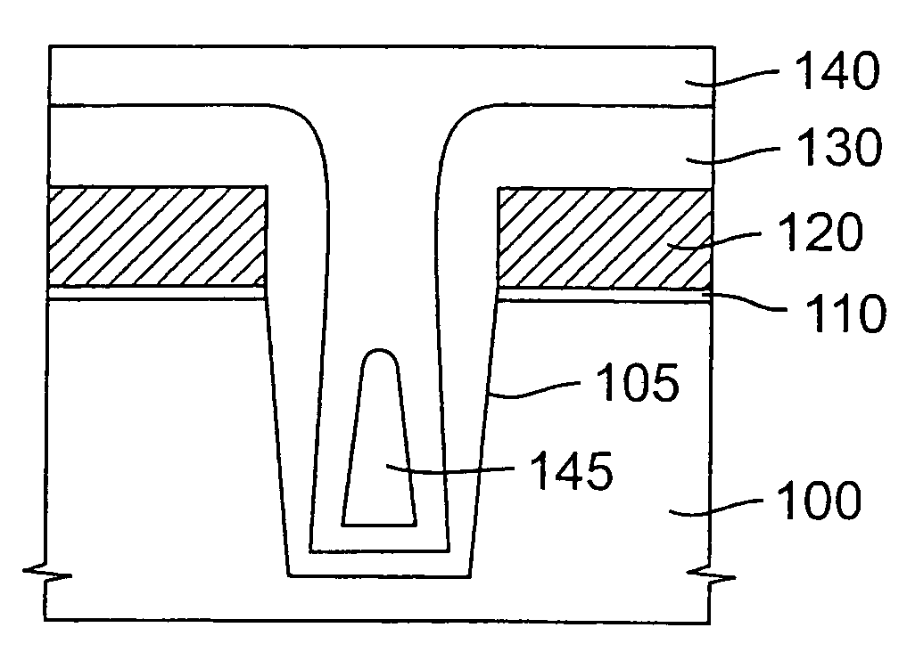
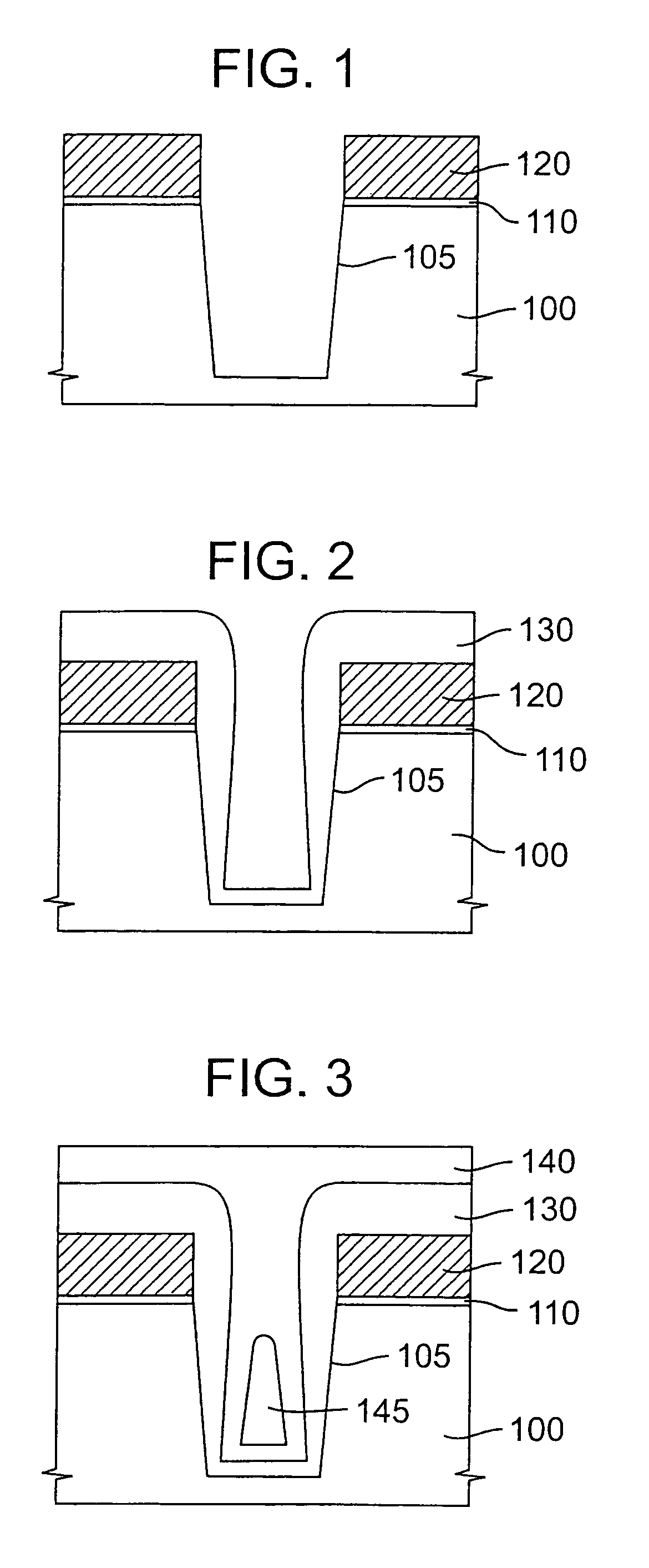
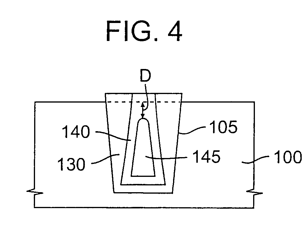
[0018]FIGS. 1 to 4 schematically show cross-sectional views of the process steps of a method of forming STI in a semiconductor substrate according to an embodiment of the present invention.

[0019]Referring to FIG. 1, a pad oxide layer is formed on a semiconductor substrate 100 such as a silicon substrate. Then, a silicon nitride layer is f...


PUM


Abstract

A shallow trench isolation (STI) structure in a semiconductor substrate and a method for forming the same are provided. A trench is formed in a semiconductor substrate. A first dielectric layer is formed on sidewalls of the trench. The first dielectric layer is formed thicker at a top portion of the sidewalls than a bottom portion of the sidewalls and leaving an entrance of the trench open to expose the trench. A second dielectric layer is conformally formed on the first dielectric layer to close the entrance, thus forming a void buried within the trench. Thus, the stress between the trench dielectric layer and the surrounding silicon substrate during thermal cycling can be substantially reduced.

Description

[0001]This application is a divisional of application Ser. No. 10 / 251,550, filed Sep. 20, 2002, now U.S. Pat. No. 6,791,155.BACKGROUND OF THE INVENTION[0002]1. Field of the Invention[0003]The present invention relates to the field of semiconductor manufacturing and, more particularly, to a stress-relieved shallow trench isolation (STI) structure and a method for fabricating the same.[0004]2. Description of the Related Art[0005]The fabrication of integrated circuits typically involves placing numerous devices on a single semiconductor substrate such as a silicon substrate. Isolation structures are used to electrically isolate one device from another. Individual devices are then interconnected by forming conducting lines over the isolation structures.[0006]Among these isolation structures, a Shallow Trench Isolation (STI) structure has become popular because the device isolation area is small, and hence the resulting trench can be well adapted for device miniaturization. Typically, ST...

Claims


Application Information

Patent Timeline
Patent Type & Authority Patents(United States)
IPC IPC(8): H01L21/76H01L21/762H01L21/764
CPCH01L21/764H01L21/76224
Inventor LO, GUO-QIANG PATRICKSCHORR, BRIANFOLEY, GARYLEE, SHIH-KED
Owner INTEGRATED DEVICE TECH INC
Why Eureka
Try Eureka