Piezoelectric device and manufacturing method therefor

a piezoelectric device and manufacturing method technology, applied in the direction of solid-state devices, generators/motors, basic electric elements, etc., can solve the problems of low adhesive strength of conventional piezoelectric devices to gold components in mounting electrodes, insufficient bonding force to resins, etc., to achieve the effect of enhancing electrical conductan

Inactive Publication Date: 2006-03-21
SEIKO EPSON CORP
View PDF18 Cites 13 Cited by
  • Summary
  • Abstract
  • Description
  • Claims
  • Application Information

AI Technical Summary

Benefits of technology

[0043]An object of the present invention is to provide a piezoelectric device having a structure which can solve the problems described above, which resists impact from the exterior of the device and stress applied to the piezoelectric resonator element, and which can enhance the electrical conductance between the electrode side of the package base and the piezoelectric resonator element.
[0045]According to this structure, since the mounting electrodes are provided with the anchor members on the surfaces thereof, when the silicone-based conductive adhesives are applied over the anchor members, the adhesive strength is enhanced compared to the conventional case in which the silicone-based conductive adhesives are directly applied over the surfaces of the electrodes. In this connection, the anchor member is a member mainly having a roughened surface or a finely irregular surface, and a member which serves to enhance an anchor effect of an adhesive. As a result, the silicone-based conductive adhesive is not adhered to a conventional electrode surface having poor adhesion and instead is adhered to, for example, the surface of the anchor member having an irregularity thereon. In the case described above, since the silicone resin penetrates into the fine irregularity of the anchor member, the adhesive strength thereof is enhanced, and in addition, since a silver filler contained in the adhesive penetrates into the fine irregularity of the anchor member, the electrical conductance is also enhanced.
[0050]Accordingly, as a result, the silicone-based conductive adhesive is not adhered to a conventional electrode surface having poor adhesion, and instead is adhered to, for example, the surface of the anchor member having an irregularity thereon. In the case described above, since the silicone resin penetrates into the fine irregularity of the anchor member, the adhesive strength thereof is enhanced, and in addition, since a silver filler contained in the adhesive penetrates into the fine irregularity of the anchor member, the electrical conductance is also enhanced.

Problems solved by technology

In this connection, the conventional piezoelectric device has a problem described below.
However, the silicone-based conductive adhesive 15 has a problem in that adhesive strength thereof adhered to the gold component in the mounting electrode is low.
That is, gold is an inert metal, is unlikely to be oxidized, and has an insufficient bonding force to a resin used for the adhesive.
In addition to this, since the shrinkage of the silicone-based conductive adhesive is low when cured by heating (ST3 in FIG. 9), the silver filler component contained therein has a weak force penetrating into the surface of the gold on the mounting electrode 14, and hence, an electrical conductance defect may occur in some cases.
Furthermore, the silicone-based conductive adhesive 15 may form a resinous layer at the interface with the gold in some cases, and as a result, the electrical conductance defect may also occur in some cases.

Method used


Image

  • Piezoelectric device and manufacturing method therefor
  • Piezoelectric device and manufacturing method therefor
  • Piezoelectric device and manufacturing method therefor

Examples


first embodiment

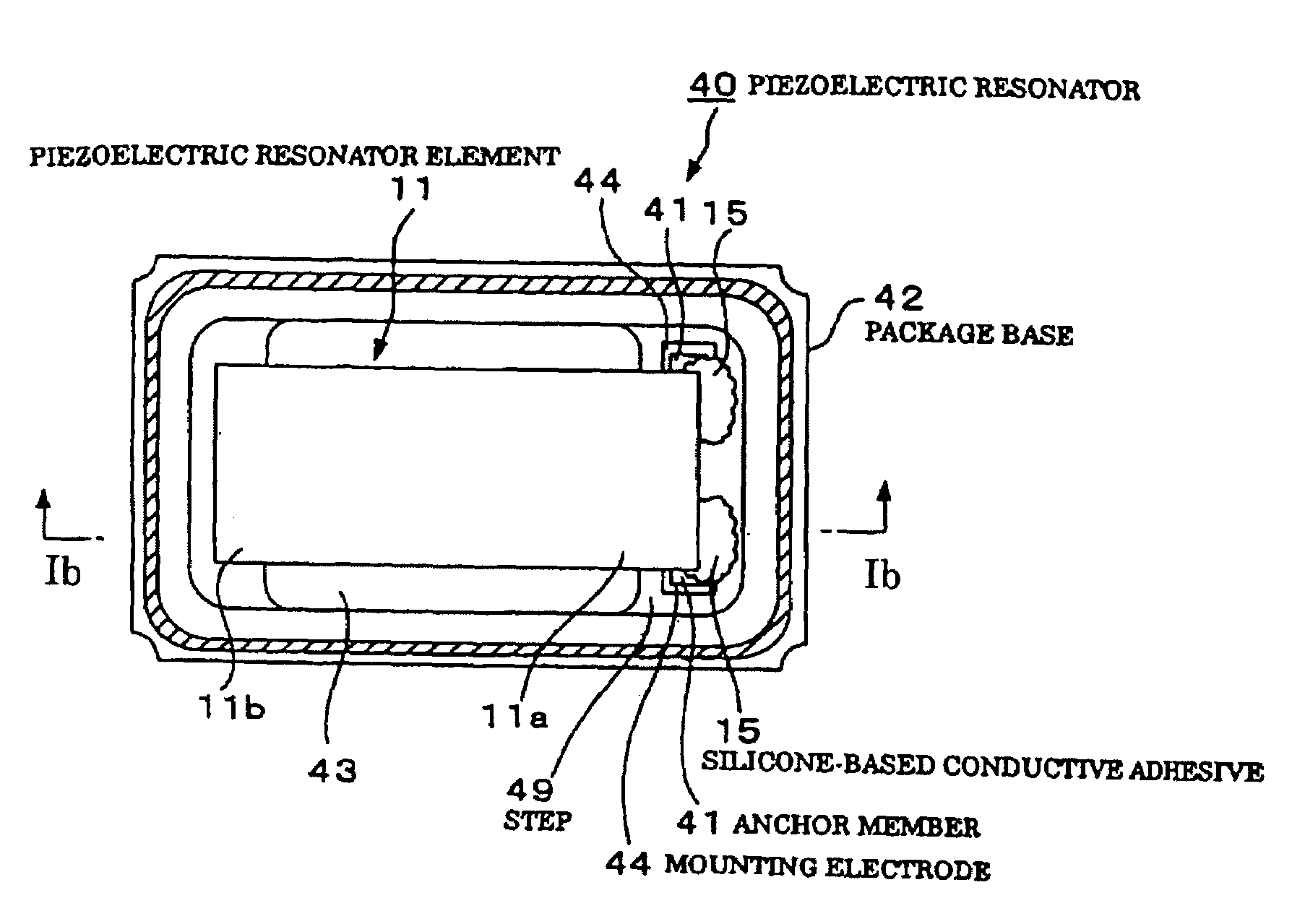
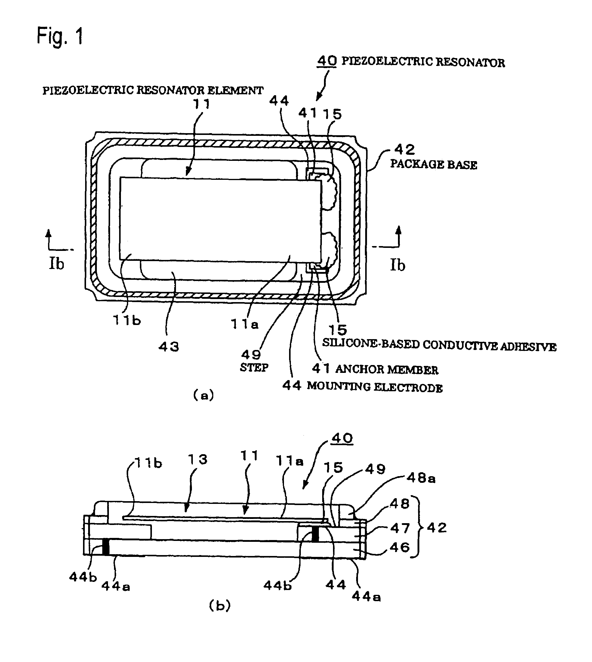
[0067]FIGS. 1(a) and 1(b) show a piezoelectric resonator as an example of a piezoelectric device to which the present invention is applied.

[0068]In FIGS. 1(a) and 1(b), for the convenience of understanding, a lid body is omitted in the figures. FIG. 1(a) is a plan view showing the interior of the piezoelectric resonator by removing the lid body, and FIG. 1(b) is a schematic cross-sectional view showing the interior taken along plane Ib—Ib (shown in FIG. 1(a)) by removing the lid body.

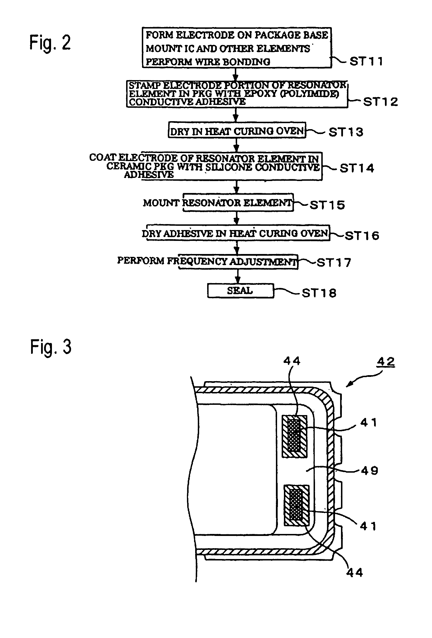
[0069]In FIGS. 1(a) and 1(b), a piezoelectric resonator 40 has a package base 42, in the form of a box, in which a space portion 43 is formed that accommodates a piezoelectric resonator element 11 in the form of a plate. One end 11a of the piezoelectric resonator element 11 is fixed on two mounting electrodes 44 and 44, disposed on a step 49 formed in the space portion 43, by bonding using silicone-based conductive adhesives 15 and 15 provided therebetween, and the other end 11b is a free end.

[0070]In t...

second embodiment

[0107]Next, a second embodiment of a piezoelectric oscillator to which the present invention is applied will be described.

[0108]Most of the features of the manufacturing steps described in the first embodiment are also equivalent to those of another device, i.e., the piezoelectric oscillator. That is, unlike the piezoelectric resonator, the piezoelectric oscillator has an integrated circuit mounted in the package base, and accordingly, the structure and the manufacturing steps thereof are slightly different from those of the piezoelectric resonator.

[0109]FIGS. 6(a) and 6(b) show a piezoelectric oscillator of the embodiment to which the present invention is applied, and for the convenience of understanding, a lid body is omitted in the figures. FIG. 6(a) is a plan view showing the interior of the piezoelectric oscillator by removing the lid body, and FIG. 6(b) is a schematic cross-sectional view showing the interior taken along plane VIb—VIb (shown in FIG. 6(a)) by removing the lid b...


PUM


Abstract

The invention provides a piezoelectric device having a structure which resists impact from the exterior of the device, and stress applied to a piezoelectric resonator element, and which can enhance electrical conductance between an electrode side of a package base and the piezoelectric resonator element, and to provide a manufacturing method therefor. A piezoelectric device having a structure in which a piezoelectric resonator element is bonded to electrodes provided on a package base, includes mounting electrodes, which are provided on the package base, to which a driving voltage is carried, via conduction paths, and on which the piezoelectric resonator element is mounted; and anchor members, which are disposed on the surfaces of the mounting electrodes, and which are formed of a material having superior adhesion to the surfaces thereof, in which the piezoelectric resonator element is bonded to these conductive anchor members with silicone-based conductive adhesives provided therebetween.

Description

BACKGROUND OF THE INVENTION[0001]1. Field of Invention[0002]The present invention relates to structures of piezoelectric devices, such as piezoelectric resonators or piezoelectric oscillators, having a piezoelectric resonator element received in a package. The present invention also relates to manufacturing methods therefor.[0003]2. Description of Related Art[0004]FIGS. 8(a) and 8(b) show an example of a conventional piezoelectric resonator, and for the convenience of understanding, a lid body thereof is omitted in the figures. FIG. 8(a) is a plan view showing the interior of the piezoelectric resonator by removing the lid body, and FIG. 8(b) is a schematic cross-sectional view showing the interior taken along plane VIIIb—VIIIb (shown in FIG. 8(a)) by removing the lid body.[0005]In FIGS. 8(a) and 8(b), a piezoelectric resonator 10 has a package base 12 in the form of a box in which a space portion 13 is formed for accommodating a piezoelectric resonator element 11 in the form of a p...

Claims


Application Information

Patent Timeline
Patent Type & Authority Patents(United States)
IPC IPC(8): H01L41/053H01L23/12H01L21/52H01L41/09H01L41/22H01L41/23H01L41/313H03H3/02H03H9/02H03H9/05H03H9/10
CPCH03H9/0547H03H9/1021H01L2224/45144H01L2224/48091H01L2924/3011H01L2924/00014H01L2924/00H03H9/05H10N30/88
Inventor SERIZAWA, SATOSHI
Owner SEIKO EPSON CORP
Why Eureka
Try Eureka