Organic element for electroluminescent devices
a light-emitting diode and electroluminescent technology, applied in the direction of discharge tube luminescnet screens, other domestic articles, natural mineral layered products, etc., can solve the problems of large efficiency loss, performance limitations that have not been studied as extensively, and pt-based organometallic complexes have not been widely used. to achieve good luminance efficiency
- Summary
- Abstract
- Description
- Claims
- Application Information
AI Technical Summary
Problems solved by technology
Method used
Image
Examples
synthetic example 1
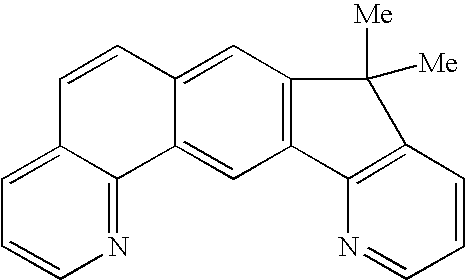
[0154]This example illustrates the preparation of the platinum complexes of the invention. The tridentate ligand 1,3-di(2-pyridyl)benzene was prepared by the following procedure. A solution of 2-bromopyridine (12.38 g, 78.4 mmol) in anhydrous THF (100 mL) was cooled with a dry ice-acetone bath and was added dropwise to a solution of n-BuLi in hexanes (53.6 mL, 1.6 M, 85.8 mmol) under nitrogen atmosphere. After addition was complete (ca. 30 min), the resultant mixture was stirred at −78 ° C. for 30 min. A solution of ZnCl2 in Et2O (50 mL, 1.0 M, 50 mmol, Aldrich) was added slowly into the reaction mixture via syringe (ca. 10 min). The dry ice-acetone bath was removed after the addition of ZnCl2 and the mixture was warmed to room temperature. Pd(PPh3)4 (1.84 g, 1.6 mmol, Aldrich) was added to the reaction mixture and followed by 1,3-dibromobenzene (6.14 g, 26 mmol). The mixture was stirred at room temperature for 3 h then refluxed for 22 h. After cooling to room temperature, the mixtu...
example 1
DEVICE EXAMPLE 1
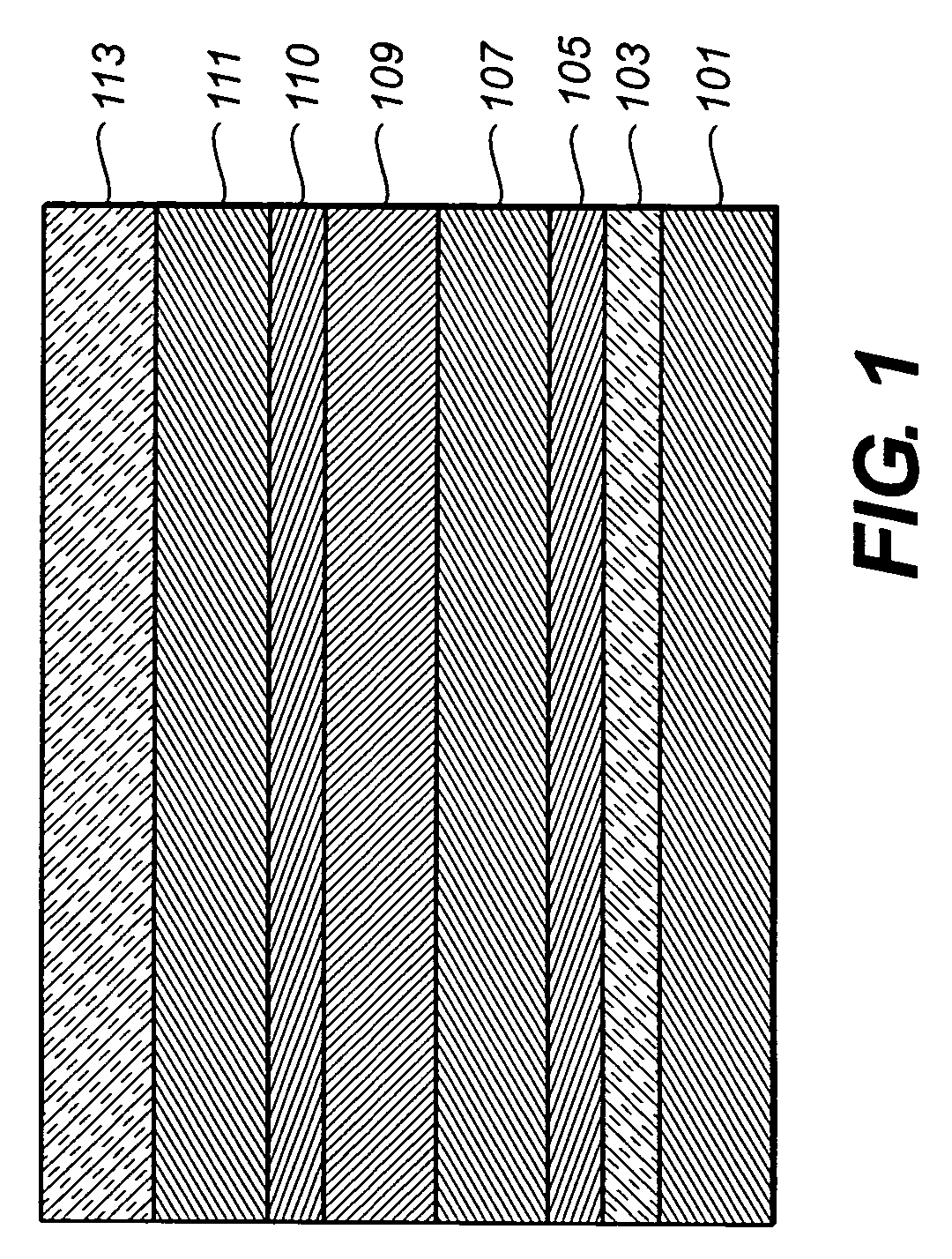
[0157]An EL device (Sample 1) satisfying the requirements of the invention was constructed in the following manner:[0158]1. A glass substrate coated with an 85 nm layer of indium-tin oxide (ITO) as the anode was sequentially ultrasonicated in a commercial detergent, rinsed in deionized water, degreased in toluene vapor and exposed to oxygen plasma for about 1 min.[0159]2. Over the ITO was deposited a 1 nm fluorocarbon (CFx) hole-injecting layer (HIL) by plasma-assisted deposition of CHF3.[0160]3. A hole-transporting layer (HTL) of N,N′-di-1-naphthyl-N,N′-diphenyl-4,4′-diaminobiphenyl (NPB) having a thickness of 75 nm was then evaporated from a tantalum boat.[0161]4. A 35 nm light-emitting layer (LEL) of 4,4′-N,N′-dicarbazole-biphenyl (CBP) and Inv-1 (2% wt %) were then deposited onto the hole-transporting layer. These materials were also evaporated from tantalum boats.[0162]5. A hole-blocking layer of bathocuproine (BCP) having a thickness of 10 nm was then evaporate...
PUM
| Property | Measurement | Unit |
|---|---|---|
| wt % | aaaaa | aaaaa |
| wt % | aaaaa | aaaaa |
| thick | aaaaa | aaaaa |
Abstract
Description
Claims
Application Information


