Methods for forming a dielectric layer within trenches

a dielectric layer and trench technology, applied in the direction of coatings, metallic material coating processes, chemical vapor deposition coatings, etc., can solve the problems of too much electrical noise, difficult to completely fill gaps and trenches in these structures without creating, and fabrication problems

Active Publication Date: 2010-09-28
APPLIED MATERIALS INC
View PDF143 Cites 432 Cited by
  • Summary
  • Abstract
  • Description
  • Claims
  • Application Information

AI Technical Summary

Problems solved by technology

While the ability to make device structures with ever increasing aspect ratios has allowed more of the structures (e.g., transistors, capacitors, diodes, etc.) to be packed onto the same surface area of a semiconductor chip substrate, it has also created fabrication problems.
One of these problems is the difficulty of completely filling the gaps and trenches in these structures without creating a void or seam during the filling process.
If the gaps were left empty, there would be too much electrical noise, and current leakage for the devices to operate properly (or at all).
As aspect ratios increased however, it became more difficult to fill the deep, narrow trench without having a blockage start a void or seam in the fill volume.
Voids and seams in a dielectric layer create problems both during semiconductor device fabrication and in the finished devices.
This results in unpredictable and inconsistent post-deposition processing of the layer, such as even etching, polishing, annealing, etc.
This can result in uneven and inferior device performance due to electrical crosstalk, charge leakage, and even shorting within and between device elements.
However, slowing the deposition rate means increasing the deposition time, which reduces processing efficiency and production rates.
However, increasing the moisture level during a silicon oxide deposition can also adversely effect the properties of the deposited film, including its density (i.e., an increased wet etch rate ratio (WERR)) and dielectric properties (i.e., an increased k-value).

Method used


Image

  • Methods for forming a dielectric layer within trenches
  • Methods for forming a dielectric layer within trenches
  • Methods for forming a dielectric layer within trenches

Examples


Embodiment Construction

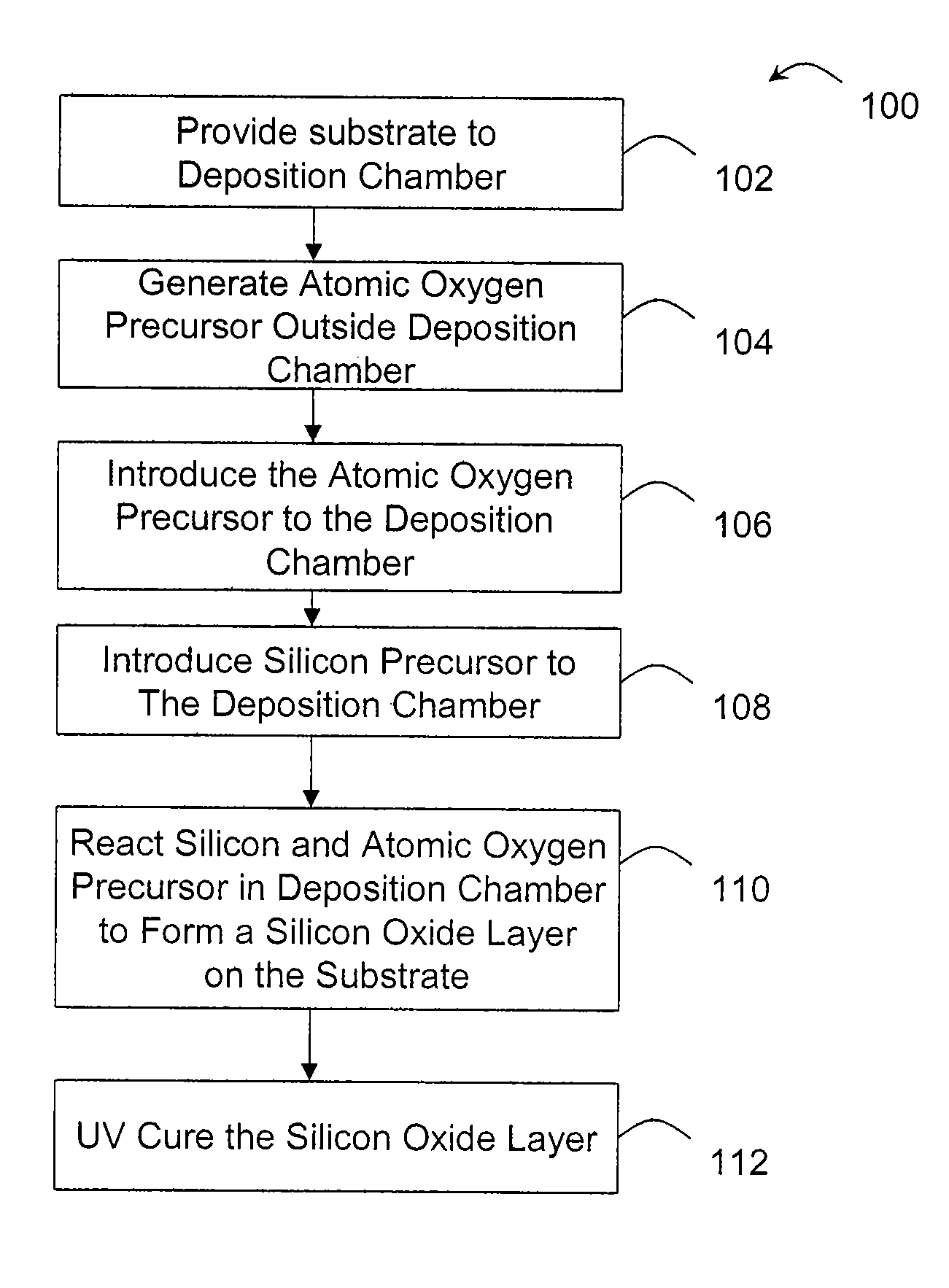
[0026]Exemplary methods are described for forming a silicon oxide layer having a desired film density, a carbon concentration and / or a wet etch rate ratio (WERR) after a UV curing within an oxygen-containing environment. The UV curing may desirably increase the density of the silicon oxide layer and / or reduce the wet etch rate ratio of the silicon oxide layer.

[0027]Some exemplary methods include reacting a silicon precursor and an atomic oxygen precursor at a processing temperature of about 150° C. or less to form a silicon oxide layer over a substrate. The silicon oxide layer is ultra-violet (UV) cured within an oxygen-containing environment. Other exemplary methods include interacting a silicon-containing precursor with at least one radical nitrogen precursor at a processing temperature of about 150° C. or less to form a silicon-nitrogen containing layer over a substrate. The silicon-containing precursor may also comprise two or more silicon atoms. The silicon-nitrogen containing ...


PUM

PropertyMeasurementUnit
temperatureaaaaaaaaaa
processing temperatureaaaaaaaaaa

Abstract

A method for forming a semiconductor structure includes reacting a silicon precursor and an atomic oxygen or nitrogen precursor at a processing temperature of about 150° C. or less to form a silicon oxide or silicon-nitrogen containing layer over a substrate. The silicon oxide or silicon-nitrogen containing layer is ultra-violet (UV) cured within an oxygen-containing environment.

Description

CROSS-REFERENCES TO RELATED APPLICATIONS[0001]This application is related to a co-assigned U.S. Patent Application and titled “CHEMICAL VAPOR DEPOSITION OF HIGH QUALITY FLOW-LIKE SILICON DIOXIDE USING A SILICON CONTAINING PRECURSOR AND ATOMIC OXYGEN.” This application is also related to a co-assigned U.S. patent application Ser. No. 11 / 754,924 by Lubomirsky et al., filed May 29, 2007, and titled “PROCESS CHAMBER FOR DIELECTRIC GAPFILL.” The application is further related to a co-assigned U.S. Patent Application and titled “HIGH QUALITY SILICON OXIDE FILMS BY REMOTE PLASMA CVD FROM DISILANE PRECURSORS.” The entire contents of the related applications are hereby incorporated by reference for all purposes.BACKGROUND OF THE INVENTION[0002]The present invention relates in general to methods for forming semiconductor structures, and more particular to methods for forming a dielectric layer within trenches.[0003]As the device density on integrated circuits continues to increase, the size a...

Claims


Application Information

Patent Timeline
Patent Type & Authority Patents(United States)
IPC IPC(8): H01L21/469
CPCC23C16/34C23C16/401C23C16/452C23C16/56H01L21/02126H01L21/02164H01L21/02167H01L21/0217H01L21/02274H01L21/02326H01L21/02337H01L21/02348H01L21/3105H01L21/31612H01L21/3185H01L21/76837H01L21/02205
Inventor LIANG, JINGMEI
Owner APPLIED MATERIALS INC
Why Eureka
Try Eureka