Method to minimize wet etch undercuts and provide pore sealing of extreme low k (k<2.5) dielectrics

a dielectric, low k (k2.5) technology, applied in the direction of resistive material coating, superimposed coating process, liquid/solution decomposition chemical coating, etc., can solve the problems of current leakage in a device, critical dimension (cd) loss, undercutting, etc., to prevent undercutting and cd loss, and minimize the wet etch rate of a low dielectric constant film

Active Publication Date: 2013-05-21
APPLIED MATERIALS INC
View PDF74 Cites 432 Cited by
  • Summary
  • Abstract
  • Description
  • Claims
  • Application Information

AI Technical Summary

Benefits of technology

The present invention provides a method for depositing a thin, conformal layer on a low dielectric constant film on a substrate, which is effective in preventing the film from being contaminated and damaged during subsequent processes. The thin layer is made of silicon and carbon, and optionally oxygen and / or nitrogen, and is deposited by reacting octamethylcyclotetrasiloxane in the presence of a low level of RF power. This layer protects the film from wet cleaning processes, such as ashing and etching, and prevents moisture adsorption onto the film. It also prevents undercuts and CD loss, and helps to recover the low dielectric constant of the film. Overall, this method improves the efficiency and reliability of a substrate manufacturing process.

Problems solved by technology

The oxidized surface of the low k films is removed during subsequent wet etch processes and contributes to undercuts and critical dimension (CD) loss.
The diffusion of barrier layer precursors into the porous low dielectric constant films results in current leakage in a device.

Method used


Image

  • Method to minimize wet etch undercuts and provide pore sealing of extreme low k (k&lt;2.5) dielectrics
  • Method to minimize wet etch undercuts and provide pore sealing of extreme low k (k&lt;2.5) dielectrics
  • Method to minimize wet etch undercuts and provide pore sealing of extreme low k (k&lt;2.5) dielectrics

Examples


Embodiment Construction

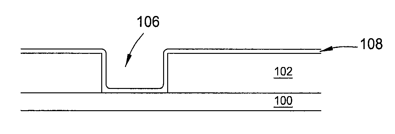
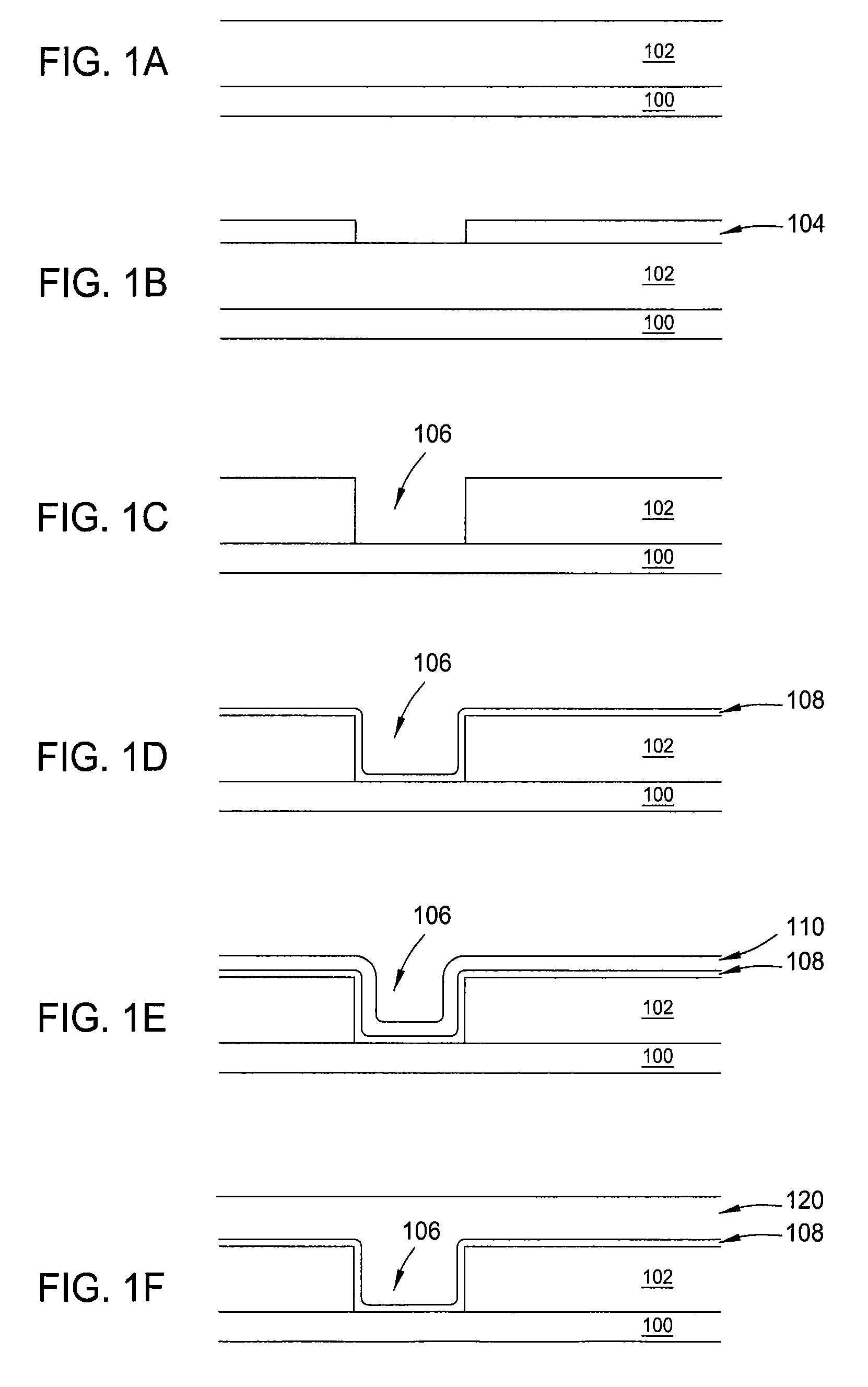
[0028]Embodiments of the present invention provide a method of depositing a thin, conformal layer comprising silicon, carbon, and optionally oxygen and / or nitrogen on a patterned substrate. In one aspect, embodiments of the present invention provide a method of protecting a patterned low dielectric constant film after a photoresist that has been used to pattern the low dielectric constant film is removed from the film. In other aspects, embodiments of the present invention provide a method of controlling the critical dimension of a metal line in an interconnect and a method of controlling the thickness of a deposited layer to between about 4 Å and about 100 Å.

[0029]In one embodiment, a low dielectric constant film on a substrate is patterned using a photoresist and photolithography to form a vertical interconnect or a horizontal interconnect opening therein. The low dielectric constant film may be a film comprising silicon, carbon, and optionally oxygen and / or nitrogen. The low diel...


PUM

PropertyMeasurementUnit
feature sizesaaaaaaaaaa
frequencyaaaaaaaaaa

Abstract

Methods of processing films on substrates are provided. In one aspect, the methods comprise treating a patterned low dielectric constant film after a photoresist is removed from the film by depositing a thin layer comprising silicon, carbon, and optionally oxygen and / or nitrogen on the film. The thin layer provides a carbon-rich, hydrophobic surface for the patterned low dielectric constant film. The thin layer also protects the low dielectric constant film from subsequent wet cleaning processes and penetration by precursors for layers that are subsequently deposited on the low dielectric constant film.

Description

CROSS-REFERENCE TO RELATED APPLICATIONS[0001]This application is a continuation of U.S. patent application Ser. No. 11 / 694,856, now abandoned, filed Mar. 30, 2007, which claims benefit of U.S. provisional patent application Ser. No. 60 / 866,770, filed Nov. 21, 2006, and is a continuation-in-part of U.S. patent application Ser. No. 11 / 668,911 now U.S. Pat. No. 7,601,651, filed on Jan. 30, 2007, which claims benefit of U.S. provisional patent application Ser. No. 60 / 790,254, filed on Apr. 7, 2006, and of U.S. provisional patent application Ser. No. 60 / 788,279, filed Mar. 31, 2006, each of which is herein incorporated by reference. Further, this application is related to U.S. patent application Ser. No. 11 / 693,005 now U.S. Pat. No. 7,780,865, filed Mar. 29, 2007.BACKGROUND OF THE INVENTION[0002]1. Field of the Invention[0003]Embodiments of the present invention generally relate to the fabrication of integrated circuits. More particularly, embodiments of the present invention relate to a...

Claims


Application Information

Patent Timeline
Patent Type & Authority Patents(United States)
IPC IPC(8): B05D3/10
CPCC23C16/308C23C16/401H01L21/02126H01L21/02164H01L21/0217H01L21/02274H01L21/0228H01L21/3122H01L21/31612H01L21/31633H01L21/76829H01L21/76831H01L21/76834H01L21/02211H01L21/02115H01L21/02203
Inventor XU, HUIWENSHEK, MEI-YEEXIA, LI-QUNAL-BAYATI, AMIRWITTY, DEREKM'SAAD, HICHEM
Owner APPLIED MATERIALS INC
Why Eureka
Try Eureka