Nitridation of high-k dielectric films

a dielectric film, high-k technology, applied in the direction of coatings, chemical vapor deposition coatings, metallic material coating processes, etc., can solve the problems of high leakage current, low mobility, and use of pure metal-oxygen compounds as gate dielectric layers, and achieve stable interface, high mobility, and promote the desired dielectric properties of the layer

Inactive Publication Date: 2005-07-14
AVIZA TECHNOLOGY INC
View PDF36 Cites 438 Cited by
  • Summary
  • Abstract
  • Description
  • Claims
  • Application Information

AI Technical Summary

Benefits of technology

[0011] In another aspect, the present invention provides a method for deposition of a multi-layer film for use as the gate dielectric in a semiconductor device. The method provides a metal-silicon-oxygen layer deposited directly on the silicon substrate where the concentration of silicon is greater than the concentration of metal so that the desired properties of high mobility and a stable interface are preserved. The method provides a second layer, deposited in-situ with the first layer, which is comprised of a metal-oxygen material, or a metal-silicon-oxygen material, where the silicon concentration is less than the metal concentration such that a dielectric layer with the highest possible “k-value” is formed to promote desired dielectric properties of the layer, such as low leakage current.
[0012] The method further provides a third layer, deposited in-situ with the first two layers, which is comprised of a metal-oxygen material or a metal-silicon-oxygen material which is then reacted with a nitrogen precursor to incorporate nitrogen into the third layer. This serves to promot...

Problems solved by technology

The thickness requirement of the gate dielectric layer is approaching equivalent oxide thickness (EOT) below 10 Å. At this thickness, electrons can “tunnel” through the SiO2 gate dielectric layer leading to excessively high leakage currents when the device is in the “off” condition.
The use of pure metal-oxygen compounds as the gate dielectric layer suffers from several issues that include low mobility (slow transistor speed), reactivity with the underlying silicon substrate, and poor diffusion blocking properties with respect to boron.
The metal-silicon-oxygen compounds are less reactive with the underlying silicon substrate and have better boron diffusion blocking properties, but suffer from lower k-values and therefore, require the deposition of thinner films.
Another problem faced in the industry is diffusion of dopants and degradation of the dielectric films during processing.
In addition, unlike the ordered interfacial network that forms between silicon and silicon dioxides, the interface between the silicon substrate and the nitr...

Method used


Image

  • Nitridation of high-k dielectric films
  • Nitridation of high-k dielectric films
  • Nitridation of high-k dielectric films

Examples


Embodiment Construction

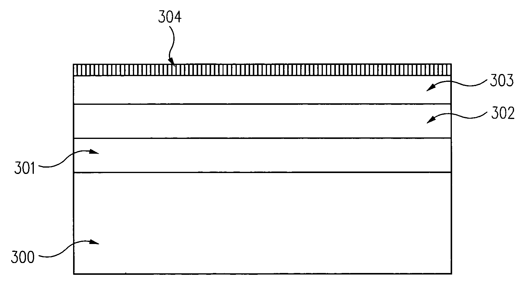
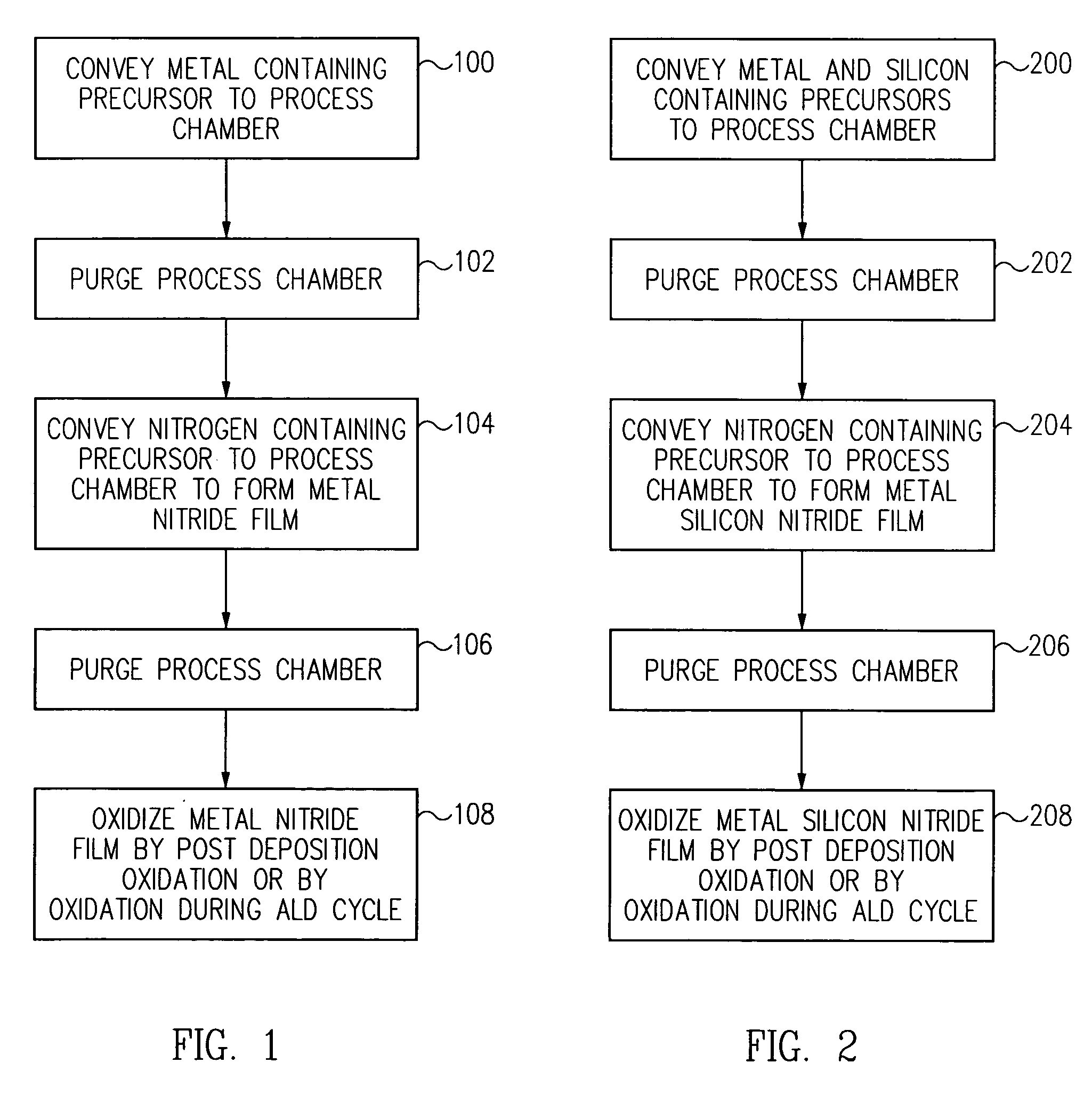
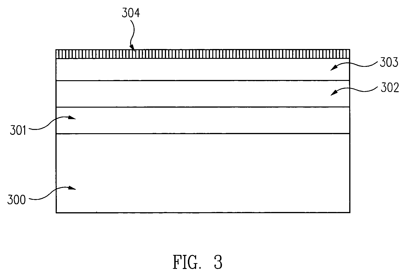
[0022] The method of the present invention promotes incorporation of nitrogen (e.g., nitridation) into high-k dielectric films using a low temperature process. Further, the present invention allows for in-situ processing, that is formation of the high-k dielectric film and nitridation of the film are carried out in the same process chamber during deposition of the film, as opposed to the conventional techniques, which carry out nitridation of the film in post processing steps.

[0023] In one aspect of the present invention, a method is provided for forming a nitrided metal oxide film by atomic layer deposition (ALD) where nitrogen is incorporated into the film during deposition. In general, an illustrative embodiment the present invention provides a method of incorporating nitrogen into high-k dielectric films by providing precursors or reactants that contain a nitridation reactant into a process chamber and carrying out atomic layer deposition (ALD) at relatively low temperatures, s...


PUM

PropertyMeasurementUnit
Temperatureaaaaaaaaaa

Abstract

The present invention promotes incorporation of nitrogen (e.g., nitridation) into high-k dielectric films using a low temperature process. Further, the present invention provides an in-situ method; that is formation of the high-k dielectric film and nitridation of the film are carried out in the same process chamber during deposition of the film, as opposed to the conventional post processing techniques. In another aspect, a method for depositing a multi-layer material for use as a gate dielectric layer in semiconductor devices is provided.

Description

RELATED APPLICATIONS [0001] The present invention claims the benefit of, and priority to, U.S. Provisional Patent Application Ser. No. 60 / 520,964, filed on Nov. 17, 2003, entitled: ALD of HiSiON with Controlled Thickness and Compositional Gradient, the entire disclosure of which is hereby incorporated by reference. The present invention is related to pending U.S. patent application Ser. No. 10 / 869,770 filed on Jun. 15, 2004, which is a CIP application of U.S. patent application Ser. No. 10 / 829,781 filed on Apr. 21, 2204, the disclosures of both of which are hereby incorporated by reference in their entirety.FIELD OF THE INVENTION [0002] The present invention relates generally to formation of dielectric films having high dielectric constant (high-k) for use in semiconductor substrates and wafers. More specifically, the present invention relates to incorporation of nitrogen into high-k dielectric films at low temperatures. BACKGROUND OF THE INVENTION [0003] Advances in semiconductor d...

Claims


Application Information

Patent Timeline
IPC IPC(8): C23C16/02C23C16/30C23C16/40C23C16/44C23C16/455H01L21/314H01L21/316
CPCC23C16/029C23C16/308C23C16/401C23C16/45531H01L21/3141H01L21/31645H01L21/3143H01L21/3145H01L21/31608H01L21/31612H01L21/3142H01L21/02148H01L21/02205H01L21/02219H01L21/0228H01L21/20H01L21/02329H01L21/02337
Inventor SENZAKI, YOSHIHIDE
Owner AVIZA TECHNOLOGY INC
Why Eureka
Try Eureka