Minimally-patterned semiconductor devices for display applications

a semiconductor device and display technology, applied in the field of electronic displays, can solve the problems of high manufacturing cost, high cost of thin-film transistors, and significant cost, and achieve the effects of increasing manufacturing cost, increasing manufacturing cost, and increasing manufacturing cos

Inactive Publication Date: 2006-04-18
E INK CORPORATION
View PDF263 Cites 379 Cited by
  • Summary
  • Abstract
  • Description
  • Claims
  • Application Information

AI Technical Summary

Benefits of technology

[0012]In still another aspect, an array of thin-film transistors that comprises at least a first transistor and a second transistor is manufactured by a method that comprises the steps of: providing a substrate; forming an unpatterned semiconductor layer, the semiconductor layer adjacent to the substrate; forming at least one patterned drain electrode for each of the transistors, the drain electrodes in electrical communication with the semiconductor layer; for

Problems solved by technology

These processes, however, can result in significant cost.
The high cost in manufacturing thin-film transistors results in part from the patterning steps, which require the use of expensi

Method used


Image

  • Minimally-patterned semiconductor devices for display applications
  • Minimally-patterned semiconductor devices for display applications
  • Minimally-patterned semiconductor devices for display applications

Examples


Embodiment Construction

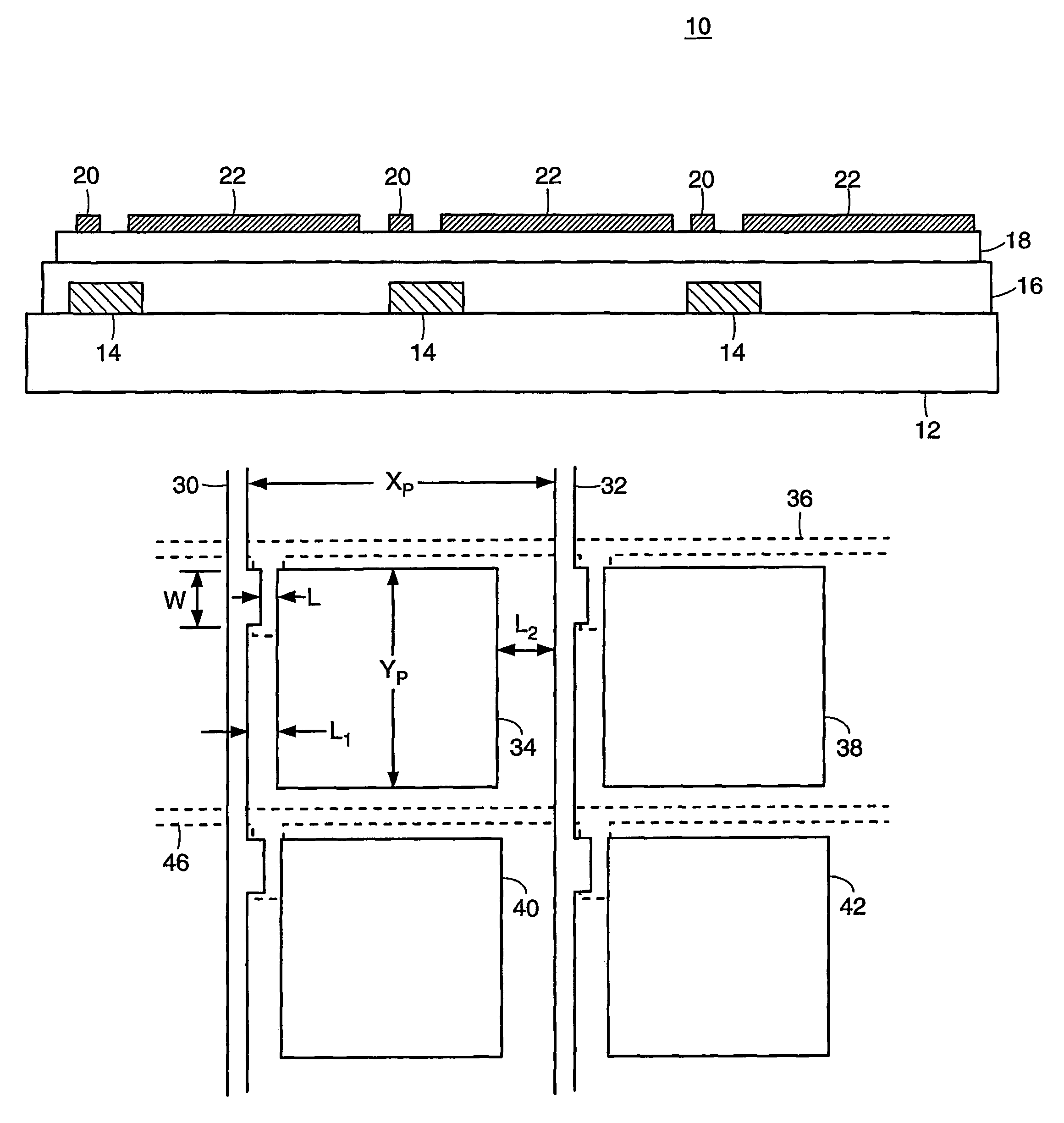
[0029]In one aspect, the invention features minimally-patterned semiconductor devices for display applications. In a preferred embodiment, the semiconductor devices are an array of thin-film transistors. Referring to FIG. 1, an array of transistors 10 include a substrate 12, a gate electrode 14 for each transistor provided adjacent to the substrate 12, a gate dielectric layer 16 provided adjacent to the substrate 12 and the gate electrodes 14, a semiconductor layer 18 provided adjacent to the gate dielectric layer 16, and a source electrode 20 and a drain electrode 22 for each transistor provided adjacent to the semiconductor layer 18.

[0030]For fabrication of thin-film transistors, the substrate 12 can be, for example: a silicon wafer; a glass plate; a steel foil; or a plastic sheet. The gate electrodes 14, for example, can be any conductive material such as metal or conductive polymer. The materials for use as the semiconductor layer 18, for example, can be inorganic materials such...


PUM


Abstract

A thin-film transistor array comprises at least first and second transistors. Each transistor comprises a source electrode, a drain electrode a semiconductor electrode, a gate electrode, and a semiconductor layer. The semiconductor layer is continuous between the first and second transistors. The semiconductor layer is preferably unpatterned. In various display applications, the geometry of the transistors is selected to provide acceptable leakage currents. In a preferred embodiment, the transistor array is employed in an encapsulated electrophoretic display.

Description

RELATED APPLICATIONS[0001]This application claims priority to provisional application U.S. Ser. No. 60 / 132,642 filed on May 5, 1999, the entire contents of which are incorporated herein by reference.FIELD OF THE INVENTION[0002]The present invention relates generally to electronic displays and methods of manufacturing the electronic displays, and more particularly to, semiconductor devices for electronic display applications and methods of manufacturing the semiconductor devices.BACKGROUND OF THE INVENTION[0003]Encapsulated, particle-based displays offer a useful means of creating electronic displays. There exist many versions of encapsulated particle-based displays including encapsulated electrophoretic displays, encapsulated suspended particle displays, and rotating ball displays.[0004]Encapsulated, particle-based displays can be made highly reflective, bistable, and optically and electrically efficient. To obtain a high-resolution display, however, individual pixels of a display m...

Claims


Application Information

Patent Timeline
IPC IPC(8): H01L29/04
CPCH01L27/1255H01L29/0603
Inventor DRZAIC, PAUL S.AMUNDSON, KARL R.DUTHALER, GREGG M.KAZLAS, PETER T.CHEN, YU
Owner E INK CORPORATION
Why Eureka
Try Eureka