Photoelectric Converter and Semiconductor Electrode

a technology of photoelectric converter and semiconductor electrode, which is applied in the direction of electrochemical generator, cell components, electrolytic capacitors, etc., can solve the problems of global and local environmental problems, radiation contamination, and global warming, and achieve the effects of increasing specific surface area, and increasing specific surface area

Inactive Publication Date: 2009-01-08
SONY CORP
View PDF10 Cites 34 Cited by
  • Summary
  • Abstract
  • Description
  • Claims
  • Application Information

AI Technical Summary

Benefits of technology

[0017]The present invention is directed to a photoelectric converter of the type having a transparent substrate, at least a semiconductor electrode formed thereon which is a layer of semiconductor fine particles, a counter electrode, and an electrolyte layer held between said semiconductor electrode and said counter electrode, wherein said layer of semiconductor fine particles is one which is prepared by forming a film from semiconductor fine particles on said transparent substrate and subsequently subjecting the resulting film to hydrothermal treatment in an environment of pH 10 or higher, so that the semiconductor fine particles have an increased specific surface area.
[0018]The semiconductor electrode according to the present invention is composed of a transparent substrate and at least a layer of semiconductor fine particles formed thereon. The layer of semiconductor fine particles, which has been formed on the transparent substrate, undergoes hydrothermal treatment, so that the semiconductor fine particles have an increased specific surface area.
[0019]According to the present invention, the layer of semiconductor fine particles constituting the semiconductor electrode undergoes hydrothermal treatment, so that the semiconductor fine particles have an increased specific surface area. The increased specific surface area permits the sensitizing dye to be supported more than before. Thus the resulting photoelectric converter has an improved photoelectric converting efficiency and an increased current density.

Problems solved by technology

It is said that fossil fuel (such as coal and petroleum) as an energy source emits carbon dioxide which results in global warming.
It is feared that nuclear power might cause contamination with radiation.
The global and local environmental problems will become more serious if man continues to depend on the conventional energies for their living and economic activity.
However, crystalline silicon needs a large amount of energy and time for crystal growth, which leads to low productivity and economical disadvantage.
On the other hand, solar cells based on amorphous silicon are inferior in conversion efficiency to solar cells based on crystalline silicon; however, the former have an advantage over the latter because of the high light absorptivity, the extensive choice of substrates, and the easy availability of large substrates.
In addition, the former are superior in productivity to the latter; however, this advantage is offset by the necessity of expensive facilities for vacuum process.
Such solar cells, however, have a very low photoelectric conversion efficiency (less than 1%) and are poor in durability.
This technique, however, does not increase the amount of the supported sensitizing dye as much as desired.
It merely gives a semiconductor electrode which is unsuitable for future photoelectric converters requiring a much higher efficiency.

Method used


Image

  • Photoelectric Converter and Semiconductor Electrode
  • Photoelectric Converter and Semiconductor Electrode

Examples


example 1

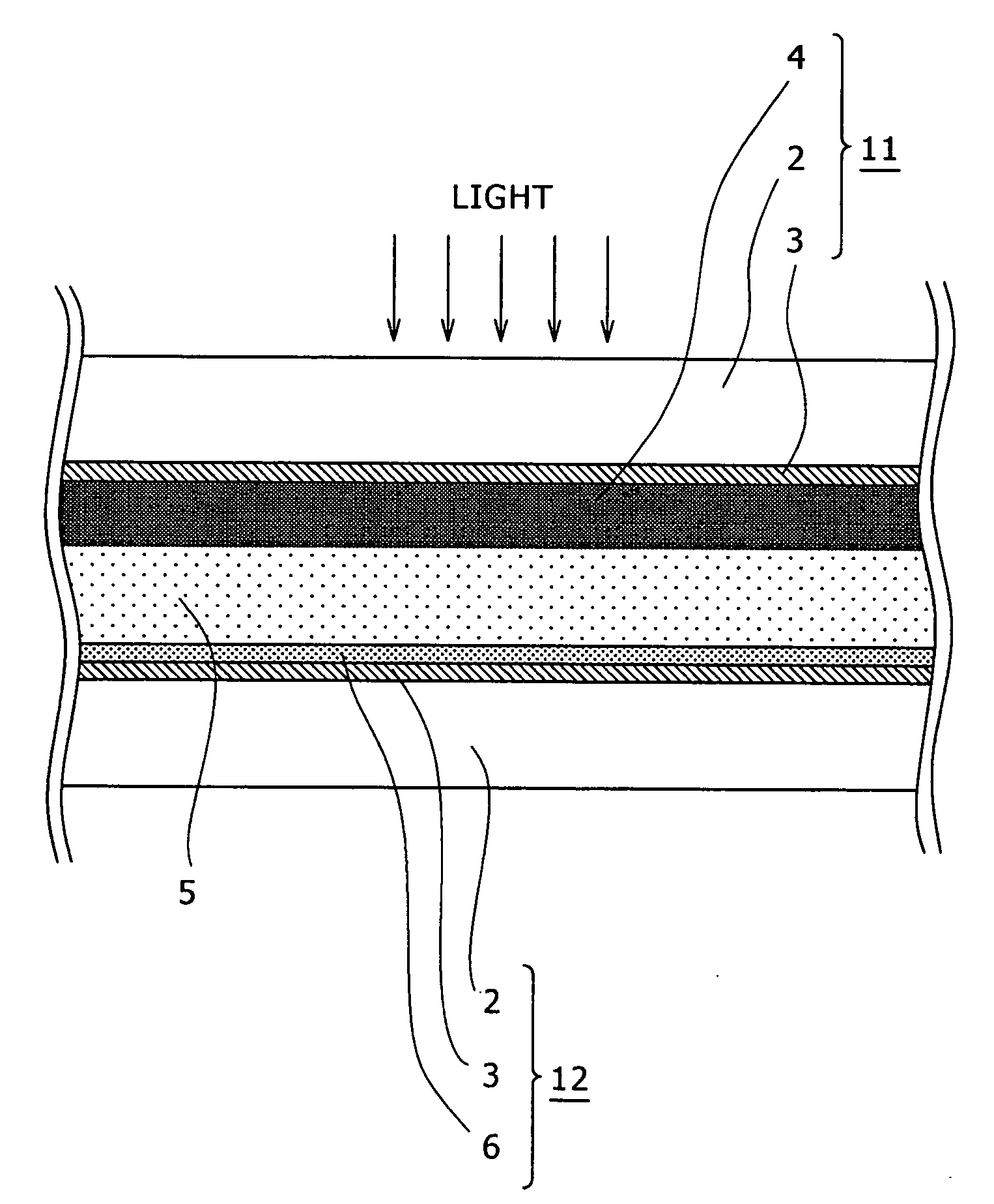
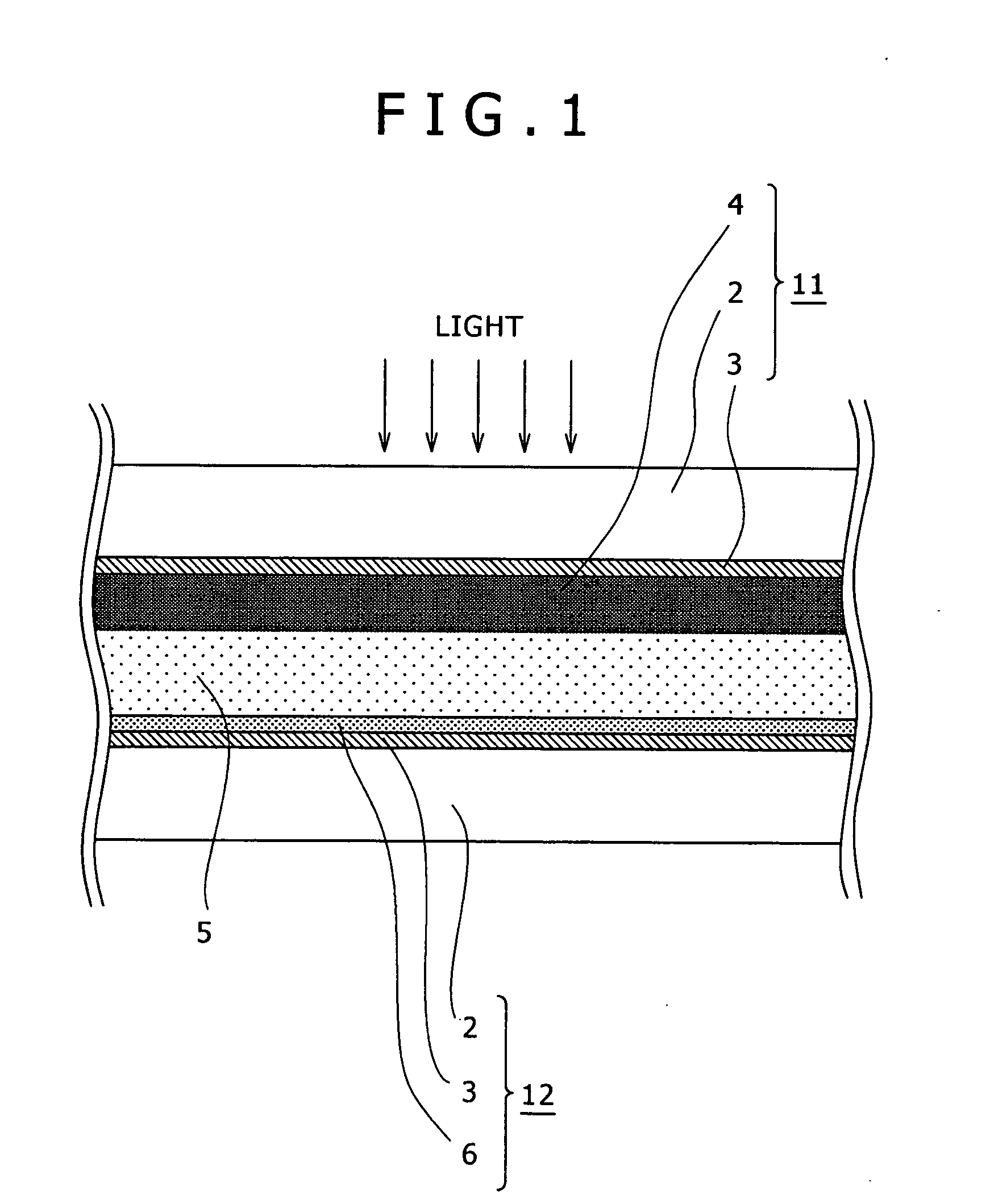
[0112]The first step was preparation of TiO2 paste for the layer of semiconductor fine particles 4.

[0113]The TiO2 paste was prepared as follows with reference to “Modern Technology of Dye-sensitized Solar Cells” issued by C.M.C.

[0114]Titanium isopropoxide (125 mL) was slowly added dropwise with stirring to 750 mL of aqueous solution of 0.1 M nitric acid at room temperature. Stirring was continued for 8 hours in a thermostat at 80° C. There was obtained a semiopaque turbid sol solution. After cooling to room temperature, this sol solution was filtered through a glass filter. Thus there was obtained 700 mL of sol solution.

[0115]The sol solution underwent hydrothermal treatment in an autoclave at 220° C. for 12 hours. The treated solution further underwent ultrasonic treatment for 1 hour to ensure dispersion. The resulting solution was concentrated by an evaporator at 40° C., so that the content of TiO2 in the concentrated solution increased to 20 wt %.

[0116]The concentrated sol soluti...

examples 2 and 3

[0128]The same procedure as in Example 1 was repeated to prepare the photoelectric converter except that the aqueous solution shown in Table 1 below was used for hydrothermal treatment of the TiO2 film constituting the layer of semiconductor fine particles.

examples 4 to 6

[0129]The same procedure as in Example 1 was repeated to prepare the photoelectric converter except that hydrothermal treatment was performed on the TiO2 film constituting the layer of semiconductor fine particles under the condition (duration of treatment) shown in Table 1 below.


PUM

PropertyMeasurementUnit
particle diameteraaaaaaaaaa

Abstract

Disclosed herein is a photoelectric converter which has an improved photoelectric conversion efficiency and an improved current density owing to the increased amount of sensitizing dye supported on the semiconductor electrode. The photoelectric converter (1) is comprised of a semiconductor electrode (11), a counter electrode (12), and an electrolyte layer (5) held between them. The semiconductor electrode (11) is comprised of a transparent substrate (2) and a layer of fine semiconductor fine particles (4). The photoelectric converter (1) is characterized in that the layer of fine semiconductor fine particles (4) undergoes hydrothermal treatment so that the semiconductor fine particles have an increased specific surface area and hence an increased amount of sensitizing dye supported thereon.

Description

TECHNICAL FIELD[0001]The present invention relates to a photoelectric converter and a semiconductor electrode suitable therefor.BACKGROUND ART[0002]It is said that fossil fuel (such as coal and petroleum) as an energy source emits carbon dioxide which results in global warming.[0003]It is feared that nuclear power might cause contamination with radiation.[0004]The global and local environmental problems will become more serious if man continues to depend on the conventional energies for their living and economic activity.[0005]Utilizing sunlight as an energy source is realized by using solar cells which are photoelectric converters to convert sunlight into electric energy. Solar cells have very little influence on the global environment and their wide spread is expected.[0006]Most commercial solar cells are made with silicon, which is classified into single crystal silicon, polycrystalline silicon, and amorphous silicon.[0007]Conventional solar cells are usually made with single cry...

Claims


Application Information

Patent Timeline
Patent Type & Authority Applications(United States)
IPC IPC(8): H01L31/00H01L31/04H01G9/20H01M14/00
CPCH01G9/2004H01G9/2031Y02E10/542H01M4/9016H01M14/005H01G9/2059Y02E60/50
Inventor MOROOKA, MASAHIRO
Owner SONY CORP
Why Eureka
Try Eureka