Photosensitized solar cell and method of manufacturing the same

a solar cell and photosensitization technology, applied in the field of photosensitized solar cells, can solve the problems of lowering efficiency and inability to ignore resistance, and achieve the effect of high energy conversion efficiency

Inactive Publication Date: 2005-05-26
KK TOSHIBA
View PDF6 Cites 33 Cited by
  • Summary
  • Abstract
  • Description
  • Claims
  • Application Information

AI Technical Summary

Problems solved by technology

Therefore, when a photosensitized solar cell having a large electrode area is fabricated, its resistance cannot be ignored, and the efficiency is lowered.

Method used


Image

  • Photosensitized solar cell and method of manufacturing the same
  • Photosensitized solar cell and method of manufacturing the same
  • Photosensitized solar cell and method of manufacturing the same

Examples


example 1

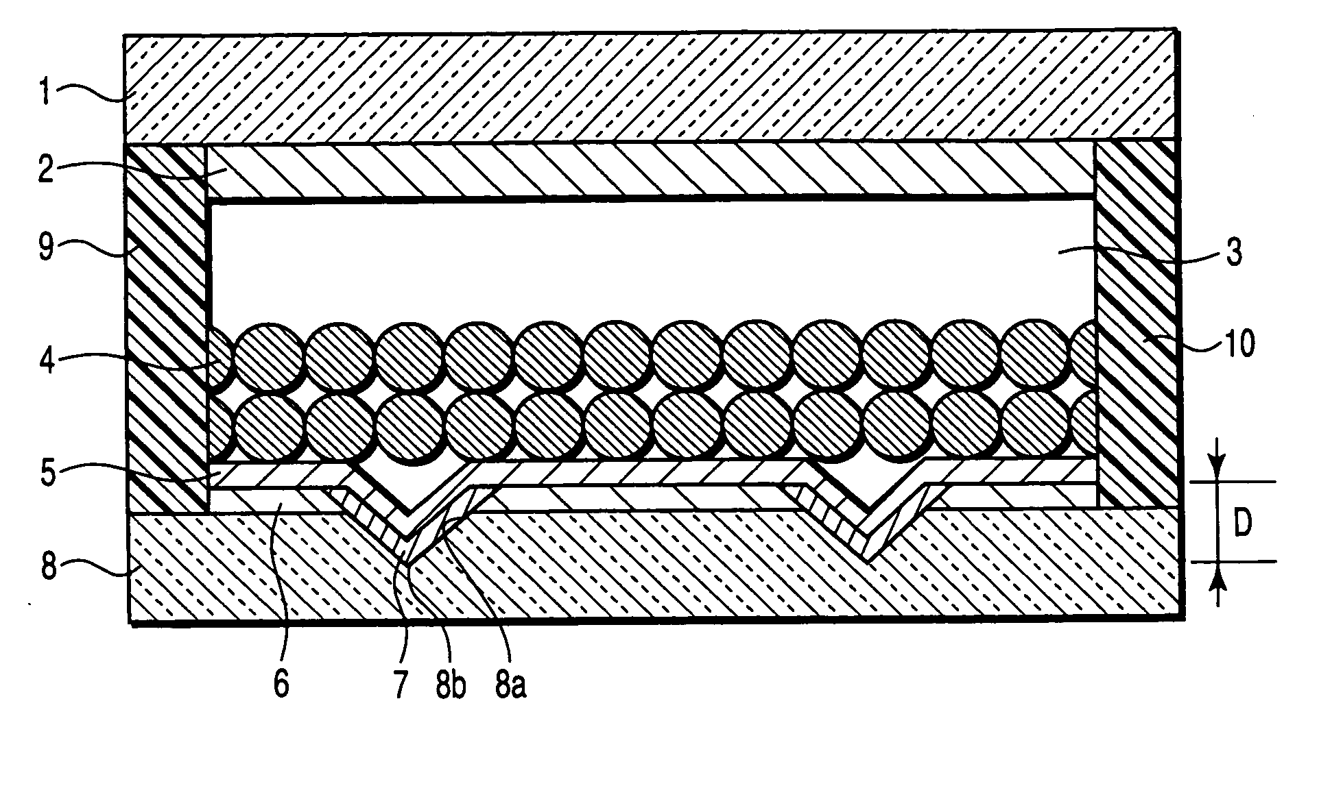
[0087] As shown in FIG. 1, on a transparent substrate 8 made of polyethylene terephthalate (PET) resin of 20 cm×15 cm size in a thickness of 100 μm, a transparent conductive oxide film (ITO) made of 90% of tin oxide and 10% of indium oxide was formed as a transparent electrode layer 6 by sputtering in a thickness of 50 nm. On the transparent electrode layer 6, a resist obtained by dissolving polyvinyl benzene in a solvent of xylene at 20% was formed by spin coating, and dried at 100° C.

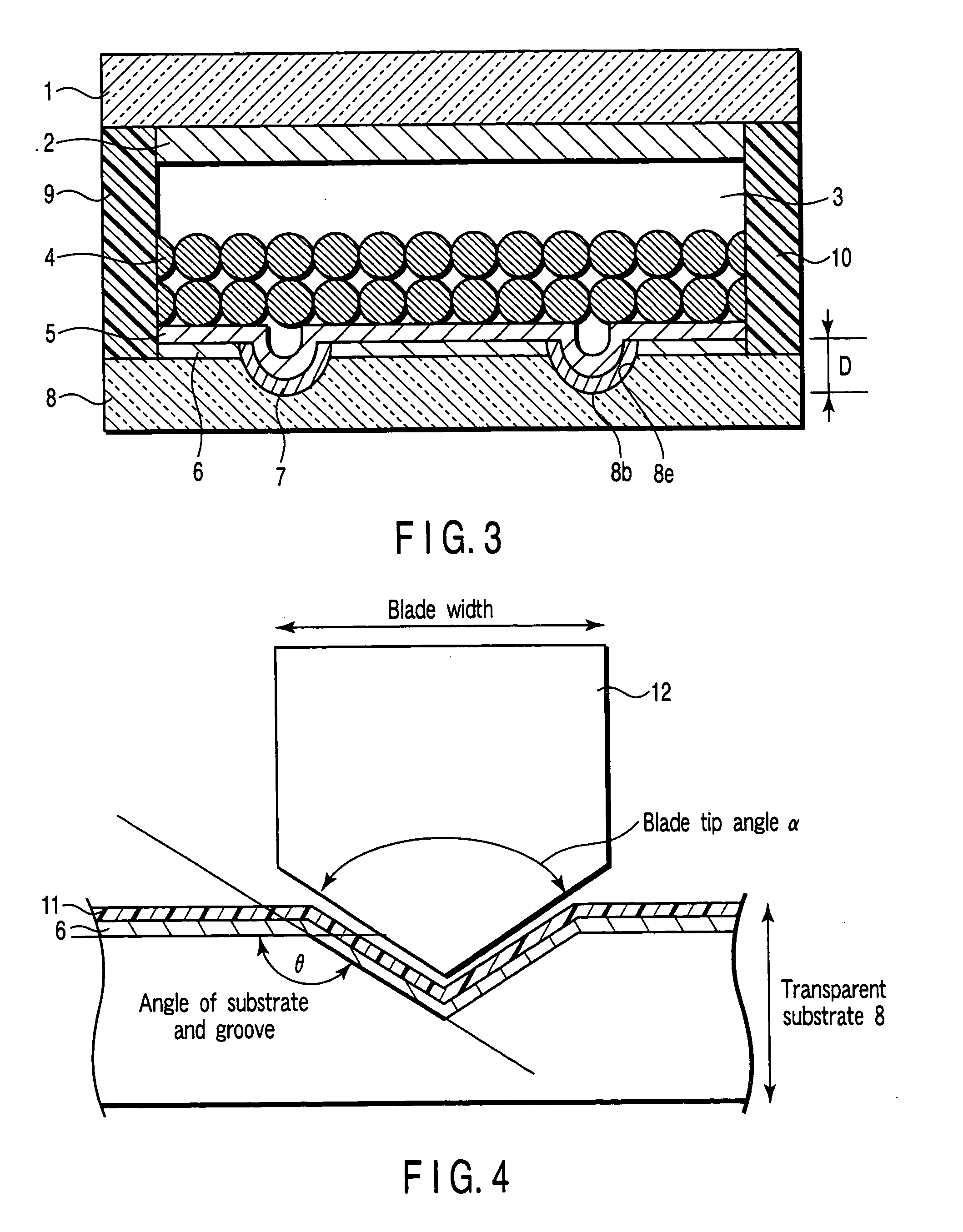
[0088] As shown in FIG. 4, mounting on a dicing saw with the side on which the transparent electrode layer 6 and resist 11 are formed upside, grooves were processed on the upper surface of the transparent substrate 8 by using a diamond blade 12 of 100 μm in thickness, having a V-form leading end whose angle α is 90 degrees. As shown in FIG. 5, the grooves 13 were formed parallel the lateral direction (shorter side direction) of the transparent substrate 6 at pitch interval L of 10 mm. Grooves interse...

example 2

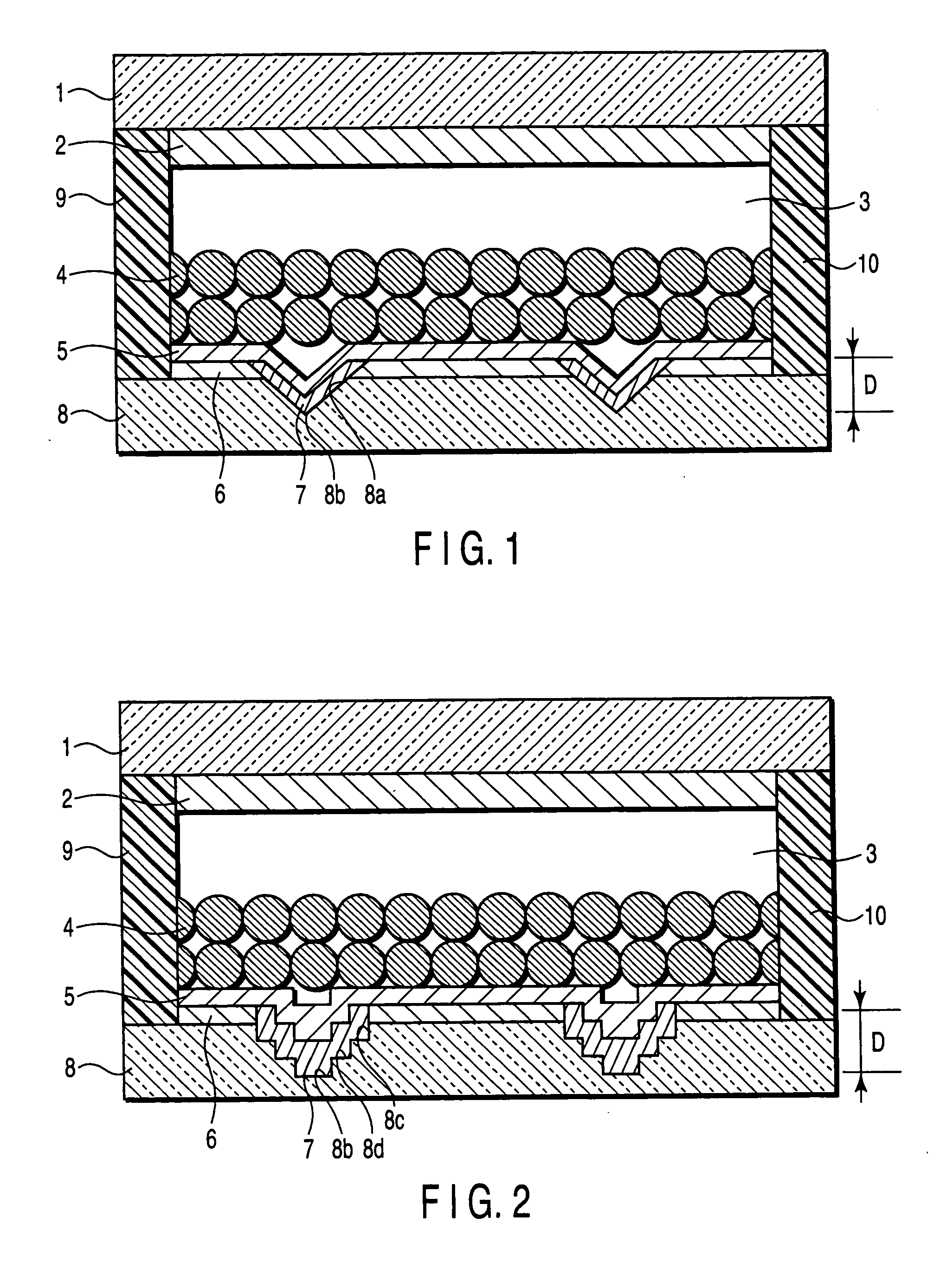
[0097] A photosensitized solar cell was manufactured by using the same materials and methods as in Example 1, except that grooves were processed in a transparent substrate 8 by using a diamond blade of 50 μm in thickness with leading end shape in stairs as shown in FIG. 2. The angle formed by the upper surface of the transparent substrate 8 and the stair section of the groove was about 135 degrees.

[0098] Similarly, when the energy conversion efficiency was measured, 3.3% was obtained. The microscopic observation of the groove disclosed peeling of the semiconductor electrode 4 of only less than 0.5% of the groove inner surface area, and the stair processing of the groove has proved improvement of peeling strength of the transparent substrate 8 and the current collector wiring 7.

example 3

[0099] A photosensitized solar cell was manufactured by using the same materials and methods as in Example 1, except that grooves were processed in a transparent substrate 8 by using a diamond blade that has a thickness of 100 μm and a U-form leading end as shown in FIG. 3. The maximum depth of the groove was 15 μm. The angle formed by the upper surface of the transparent substrate 8 and the tangent of the groove section was about 150 to 160 degrees.

[0100] Similarly, when the energy conversion efficiency was measured, 3.6% was obtained. The microscopic observation of the groove disclosed peeling of the semiconductor electrode 4 of only less than 1% of the groove inner surface area. The transparent substrate 8 was less in deflection, and the mechanical strength of the solar cell was increased by reducing the depth of the groove.


PUM


Abstract

A photosensitized solar cell includes a transparent substrate, a groove formed in a surface of the transparent substrate, and having a wall surface and a bottom surface, at least a part of the wall surface being parallel to or inclined to the surface of the transparent substrate, a current collector wiring made of metal, provided on the bottom surface and wall surface of the groove, a transparent electrode layer provided in a non-groove region on the surface of the transparent substrate, a counter substrate, a conductive layer provided on the counter substrate, a semiconductor electrode provided between the conductive layer and the transparent electrode layer, and carrying a dye, and an electrolyte layer provided between the semiconductor electrode and the conductive layer.

Description

CROSS-REFERENCE TO RELATED APPLICATIONS [0001] This application is based upon and claims the benefit of priority from prior Japanese Patent Application No. 2003-338563, filed Sep. 29, 2003, the entire contents of which are incorporated herein by reference. BACKGROUND OF THE INVENTION [0002] 1. Field of the Invention [0003] The present invention relates to a photosensitized solar cell and a method of manufacturing the same. [0004] 2. Description of the Related Art [0005] A general photosensitized solar cell comprises a transparent electrode which supports a semiconductor layer having a dye carried on a surface of fine particles of metal oxide, a counter electrode facing the transparent electrode, and an electrolyte layer interposed between the two electrodes. [0006] Such a photosensitized solar cell operates in the following process. That is, an incident light coming from the transparent electrode side reaches the dye carried on the surface of the semiconductor layer, and excites thi...

Claims


Application Information

Patent Timeline
Patent Type & Authority Applications(United States)
IPC IPC(8): H01G9/20H01L31/04H01L31/00
CPCH01G9/2004H01G9/2022Y02E10/542H01G9/2031H01G9/2095H01G9/2027Y02P70/50
Inventor KOBAYASHI, TSUYOSHI
Owner KK TOSHIBA
Why Eureka
Try Eureka