Encapsulation Module Method for Production and Use Thereof

a technology of encapsulation module and micromechanical arrangement, which is applied in the direction of electrical apparatus casing/cabinet/drawer, semiconductor/solid-state device details, electrical apparatus casing/cabinet/drawer, etc., can solve the problems of parasitic effects creeping, high temperature gradient or deficient long-term stability, and adverse effects on the parameters of components, etc., to achieve reliable and robust connection

Active Publication Date: 2010-11-18
CONTINENTAL TEVES AG & CO OHG
View PDF3 Cites 35 Cited by
  • Summary
  • Abstract
  • Description
  • Claims
  • Application Information

AI Technical Summary

Benefits of technology

[0066]Preferably, the ASIC or the encapsulation wafer or the plated-through hole wafer is used as a housing termination, in particular a housing base. An adapted thermal expansion behavior and thus a small influence of the package on the encapsulated structure under thermal loading is thereby achieved.
[0067]In order to encapsulate and/or connect two or more micromechanical modules, use is preferably made of interlayers composed of...

Problems solved by technology

On account of the contact-connection of different materials, in particular different metals and/or crystalline or amorphous silicon, adverse effects on the parameters of the components such as, for example, a high temperature gradient or a deficient long...

Method used


Image

  • Encapsulation Module Method for Production and Use Thereof
  • Encapsulation Module Method for Production and Use Thereof
  • Encapsulation Module Method for Production and Use Thereof

Examples


Embodiment Construction

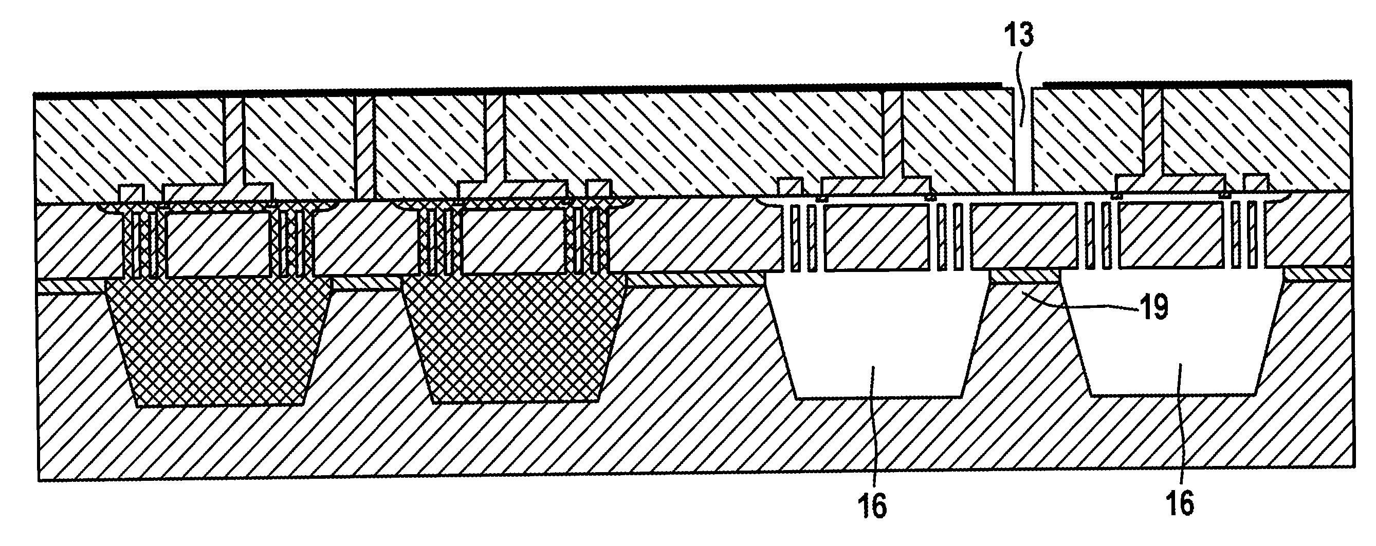
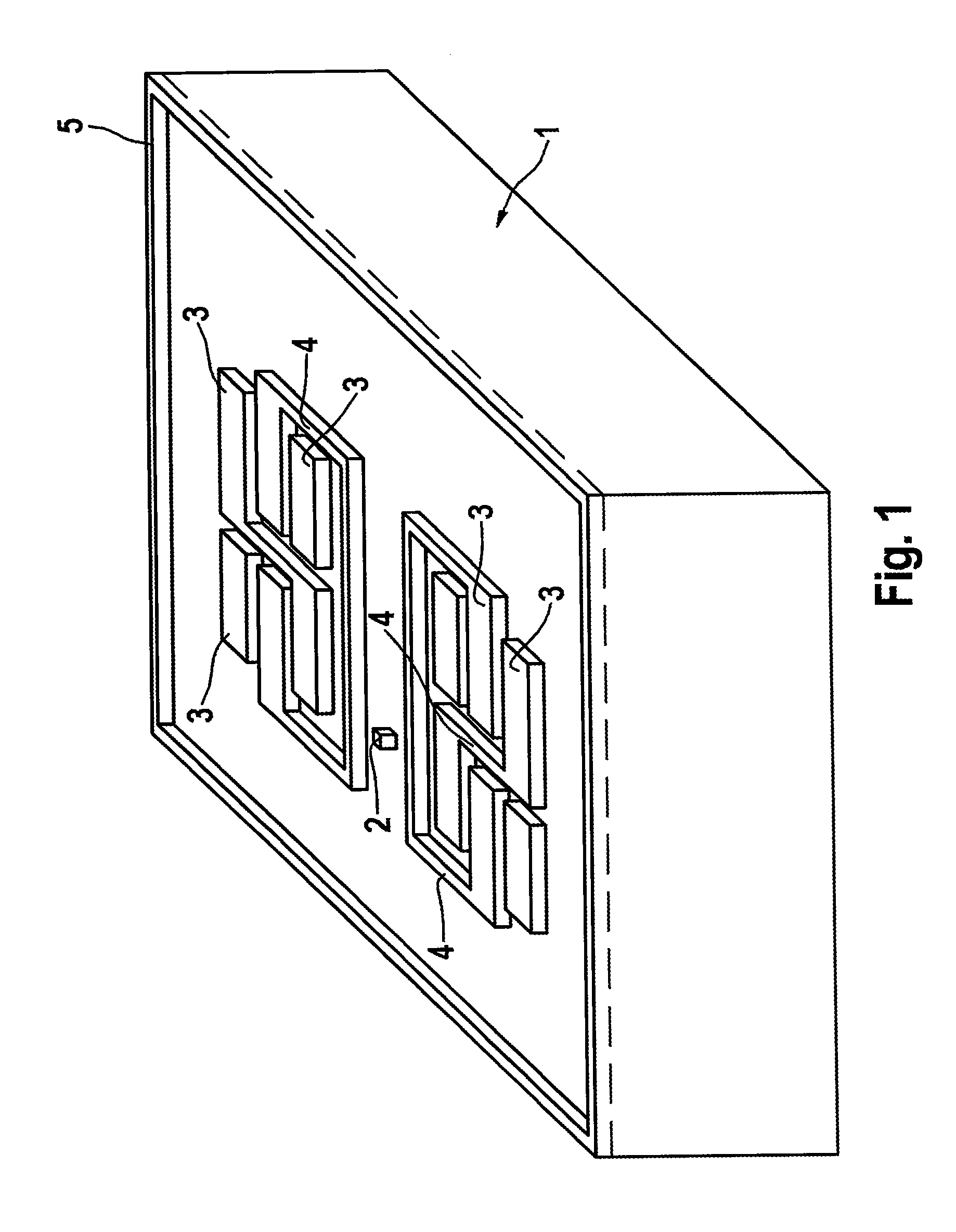
[0084]FIG. 1 shows an exemplary wafer or blank 1 composed of electrically conductive semiconductor material, in this case doped silicon, from which semiconductor material is removed by means of an etching method, whereby electronic connection means are formed. In this case, proceeding from the top surface of the wafer 1, etching is effected substantially perpendicularly downward. There are formed on the wafer by way of example semiconductor electrodes 3, semiconductor interconnects 4, which produce electrical connections between semiconductor electrodes, and also an initial formation of a plated-through hole 2 without an assigned semiconductor electrode or semiconductor interconnect as electronic connection means. Furthermore, the wafer 1 has a frame 5. Such a frame is not present in an alternative exemplary embodiment (not illustrated). Semiconductor electrodes 3 are formed substantially in insular fashion, by way of example.

[0085]In FIG. 2, the doped silicon of the wafer or blank ...


PUM


Abstract

A method for producing an encapsulation module and/or for encapsulating a micromechanical arrangement, wherein electronic connection provisions are formed from a blank of electrically conductive semiconductor material, by one or more structuring processes and/or etching processes, wherein, in the course of forming the electronic connection provisions, a pedestal of the semiconductor material arises, on which the electronic connection provisions are arranged, wherein the latter are subsequently embedded with an embedding material and the embedding material and/or the semiconductor pedestal are removed after the embedding to an extent such that a defined number of the electronic connection provisions have electrical contacts on at least one of the outer surfaces of the encapsulation module thus produced, wherein
upon forming the electronic connection provisions, on the pedestal of the semiconductor material, an insular material hump is formed, on which a plated-through hole is arranged in each case, and which embodies a semiconductor electrode.

Description

CROSS REFERENCE TO RELATED APPLICATIONS[0001]This application is the U.S. national phase application of PCT International Application No. PCT / EP2007 / 063975, filed Dec. 14, 2007, which claims priority to German Patent Application No. DE102006060794.5, filed Dec. 21, 2006 and German Patent Application No. DE102007060931.2, the contents of such applications being incorporated by reference herein.BACKGROUND OF THE INVENTION[0002]1. Field of the Invention[0003]The invention relates to an encapsulation module and / or a micromechanical arrangement, a production method, and the use of such an encapsulation module and / or of such a micromechanical arrangement in motor vehicles.[0004]2. Description of the Related Art[0005]Document EP 1 371 092 B1 proposes a planar substrate composed of glass which has perforations or feedthroughs composed of electrically conductive silicon.[0006]When such a planar substrate is used in a micromechanical arrangement, metal electrodes are usually applied to at lea...

Claims


Application Information

Patent Timeline
IPC IPC(8): H05K5/00H01L21/70H01L21/56
CPCB81B2207/012B81B2207/095H01L2924/1461B81B2207/096B81B2207/097B81C1/0023B81C1/00301H01L23/055H01L2224/73204H01L2924/01079H01L2924/1433H01L2924/01019H01L2924/01322H01L2924/00B81B7/00B81C1/00
Inventor SCHMID, BERNHARDHILSER, ROLANDKUISMA, HEIKKITORKKELI, ALTTI
Owner CONTINENTAL TEVES AG & CO OHG
Why Eureka
Try Eureka