Positional information measuring method and device, and exposure method and apparatus

a technology of positioning information and measuring method, applied in the direction of microlithography exposure apparatus, printers, instruments, etc., can solve the problems of cumbersome preparation steps (training steps), insufficient overlay accuracy, and insufficient overlay accuracy, so as to improve overlay accuracy, easy to detect relative displacement, and high accuracy

Inactive Publication Date: 2006-11-09
NIKON CORP
View PDF9 Cites 32 Cited by
  • Summary
  • Abstract
  • Description
  • Claims
  • Application Information

AI Technical Summary

Benefits of technology

[0030] Furthermore, the first mark and the second mark may be different from each other in pitch. This makes it possible to easily detect the relative displacement between the first and second marks as enlarged in a moiré pattern.
[0031] A device manufacturing method according to the present invention is a device manufacturing method including a lithography process, wherein a device pattern is transferred to a photosensitive object using the exposure method according to the present invention in the lithography process. According to the present invention, devices are manufactured with high accuracy owing to improved overlay accuracy at the time of exposure.
[0032] With the present invention, because the marks different from each other in pitch are used, when the scatterometry or reflectometry is used, it is possible to easily obtain information on the relative displacement between the two marks as enlarged for example in a moiré pattern.
[0033] The present invention also makes it possible to form in advance two marks on different layers, so as to easily measure the overlay error of the two layers without making a preparatory step in particular.
[0034] The method and apparatus for exposure according to the present invention also make it possible to carry out alignment with high accuracy using the scatterometry or reflectometry.

Problems solved by technology

Therefore, there is a drawback that cumbersome preparatory steps (training steps) are required to obtain the relationship by actually measuring the spectral reflectance on a large number of samples of different relative displacement amounts for the second layer relative to that for the first layer.
There is another drawback that, since the relationship between the variation amount of the spectral reflectance and the relative displacement varies with the layer and with the constitution of the mark, the preparatory step is required for every different process and different mark, taking in much time for evaluating the overlay error.
There is still another drawback that, since the amount of expansion or contraction of the center-to-center distance of two pairs of marks displaced by design values of +¼ pitch and −¼ pitch might also result in measurement errors, the temperature at the time of measurement must be in agreement with high accuracy with the temperature at the time of exposure.

Method used


Image

  • Positional information measuring method and device, and exposure method and apparatus
  • Positional information measuring method and device, and exposure method and apparatus
  • Positional information measuring method and device, and exposure method and apparatus

Examples


first embodiment

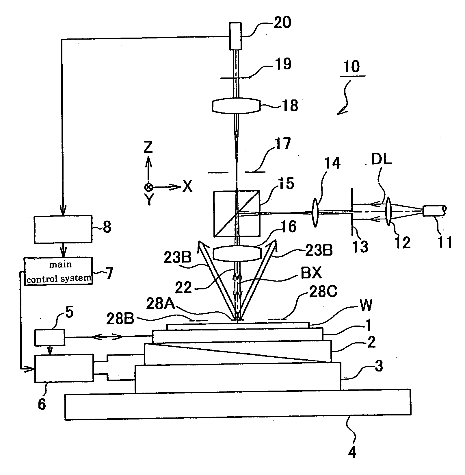
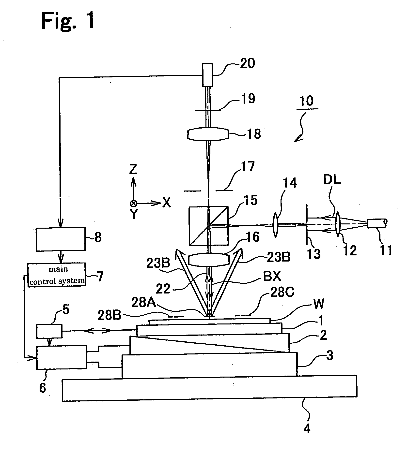
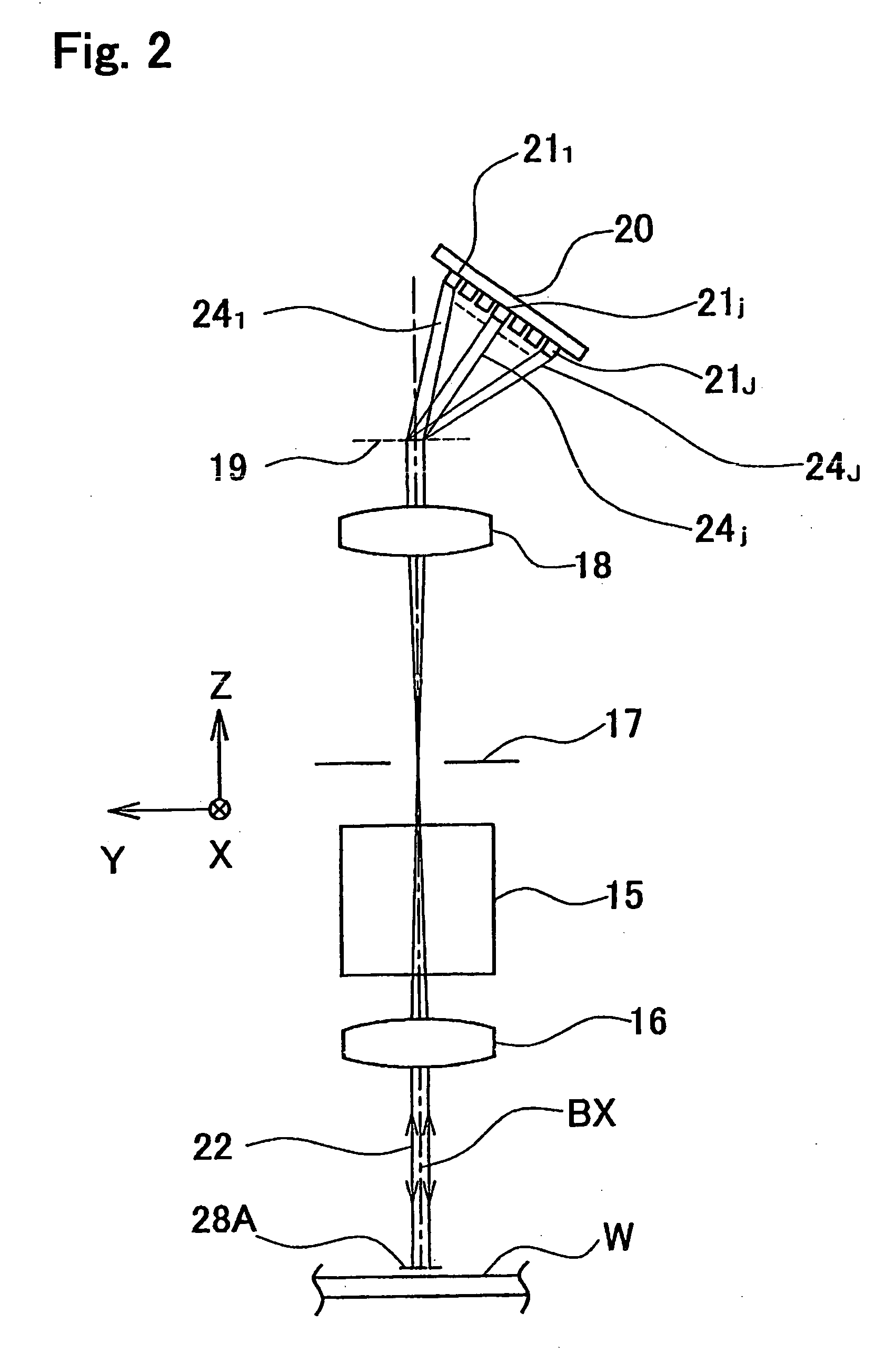
[0044] A preferable first embodiment of the present invention is described below in reference to FIGS. 1 through 3, and 9. This example is an application of the present invention to the measurement of overlay error using the reflectometry as a type of the scatterometry.

[0045]FIG. 1 shows the embodiment, an apparatus for measuring the overlay error. As shown in FIG. 1, the second marks, or marks 28A, 28B, and 28C, are formed on the upper layer of a measurement object, a wafer W. The lower layers of these marks are respectively provided with first marks (not shown, to be described later in detail). This embodiment is assumed to measure the relative displacement amount of the central mark 28A on the upper layer corresponding to the central first mark on the lower layer. Relative displacement amounts of other pair of marks are measured likewise. Incidentally, while the pairs of marks are provided in three positions in this example, their layout and number may be arbitrary. The following...

second embodiment

[0074] Next, the present invention is described in reference to FIGS. 6A and 6B. This example is the one in which two-dimensional image pickup element is used in place of the one-dimensional image pickup element 20 in the spectral reflectance detecting device 10 shown in FIG. 1. In FIGS. 6A and 6B, components corresponding to those in FIGS. 1 and 2 are provided with the same or like reference numerals and symbols, and their descriptions are not repeated.

[0075]FIG. 6A shows a spectral reflectance detecting device 10A of this embodiment. FIG. 6B is a side view of FIG. 6A. An illumination field stop 13A shown in FIGS. 6A and 6B is set to illuminate a wider area on the wafer W in comparison with the illumination field stop 13 shown in FIG. 1. That is, the detection light DL of this example illuminates an area that covers the entire width (50 μm in this example) in the measurement direction (X-direction) of the mark 28A of the second layer on the wafer W, for example an illumination area...

third embodiment

[0079] Next, the present invention is described in reference to FIG. 7. This example is an application of the invention to a case in which alignment is made using an exposure device of the proximity type.

[0080]FIG. 7 shows the exposure device of the proximity type of this example. At the time of exposure in the state shown in FIG. 7, an exposure light IL (exposure beam) from an exposure light source (not shown) for example of KrF excimer laser (of a wavelength of 248 nm) with even luminance distribution illuminates a pattern area of the pattern surface (underside) of the reticle R as a mask, through an illumination optical system 31. The illumination optical system 31 is made up of: an optical integrator for making even the luminance distribution, a field stop (reticle blind) for defining the illumination area, a condenser lens, etc.

[0081] Under the exposure light IL, a circuit pattern on the reticle R is projected to the wafer W as a substrate on which photoresist is applied. Inci...


PUM

PropertyMeasurementUnit
wavelength rangeaaaaaaaaaa
diameteraaaaaaaaaa
widthaaaaaaaaaa

Abstract

A position information measuring method capable of easily obtaining information on a relative position deviation between two marks by using scatterometry or reflectometry. Marks (25A) are formed on a wafer (W) at a pitch P1, and marks (28A) are formed on an intermediate layer (27) over them at a pitch P2 different from the pitch P1. A detection light (DL) is allowed to vertically enter the wafer (W) and a regular reflection light (22) from two marks (25A, 28A) only is spectrally separated on a wavelength basis for photoelectric converting. Wavelength-based reflectances are obtained from obtained detection signals, a reflectance at a specified wavelength is determined for each position in the measuring direction (X direction) of marks (25A, 28A), the shape of a Moire pattern formed by the overlapping of two marks (25A, 28A) is determined from the obtained reflectance distribution, and the position deviation amount of a mark (28A) is determined from the shape.

Description

TECHNICAL FIELD [0001] The present invention relates to method and device for measuring positional information, or for obtaining information on the relative displacement of two marks, using the so-called scatterometry or reflectometry. The method and device are suitable for use for example in evaluating the alignment of the mask and the circuit board in the exposure process in which the mask pattern of any device such as a semiconductor element, an image pickup element (such as CCD), or a display element (such as a liquid crystal display element) is transferred onto a substrate. The method and device are also suitable for evaluating the overlay error after the exposure. BACKGROUND ART [0002] For example in the exposure step of the lithography process for manufacturing semiconductor elements and liquid crystal display elements, an exposure device such as a stepper is used to project by exposure the image of a fine pattern formed on a reticle (or photo-mask, etc.) serving as a mask on...

Claims


Application Information

Patent Timeline
Patent Type & Authority Applications(United States)
IPC IPC(8): G03B27/52G03F7/20
CPCG03F9/7049G03F7/70633
Inventor NAKAJIMA, SHINICHI
Owner NIKON CORP
Why Eureka
Try Eureka