Display device

a display device and display technology, applied in the field of display devices, can solve problems such as display quality reduction, and achieve the effect of high display quality

Inactive Publication Date: 2014-07-03
SEMICON ENERGY LAB CO LTD
View PDF31 Cites 33 Cited by
  • Summary
  • Abstract
  • Description
  • Claims
  • Application Information

AI Technical Summary

Benefits of technology

[0011]In view of the above, an object of one embodiment of the present invention is to provide a novel eye-friendly display device or the like. An object of one embodiment of the present invention is to provide a novel display device or the like causing less eye fatigue. An object of one embodiment of the present invention is to provide a novel display device or the like without deterioration of display quality. An object of one embodiment of the present invention is to provide a novel display device or the like with little influence of off-state current. An object of one embodiment of the present invention is to provide a novel display device or the like with little influence of display degradation. An object of one embodiment of the present invention is to provide a novel display device or the like with little influence of display flickers. An object of one embodiment of the present invention is to provide a novel display device or the like with less variation in display luminance. An object of one embodiment of the present invention is to provide a novel display device or the like capable of displaying a clear still image. An object of one embodiment of the present invention is to provide a novel display device or the like with low power consumption. An object of one embodiment of the present invention is to provide a novel display device or the like with little deterioration of a transistor. An object of one embodiment of the present invention is to provide a novel display device or the like including a transistor with low off-state current. An object of one embodiment of the present invention is to provide a novel display device or the like.
[0014]With one embodiment of the present invention, a novel display device with high display quality can be provided.

Problems solved by technology

Once the amount of change in voltage written into a pixel exceeds an amount corresponding to the allowable variation range of gray level in one image (still image), a user perceives a flicker of the image, resulting in a reduction in display quality.

Method used


Image

  • Display device
  • Display device
  • Display device

Examples


embodiment 1

[0057]In this embodiment, a structure and a driving method of a display portion included in the display device of one embodiment of the present invention will be described with reference to FIGS. 1A to 1C, FIG. 2, FIG. 3, FIG. 4, FIG. 5, FIG. 6, FIG. 7, FIG. 8, and FIG. 9. Note that in this embodiment, as a display device, a liquid crystal display device including a liquid crystal element is described.

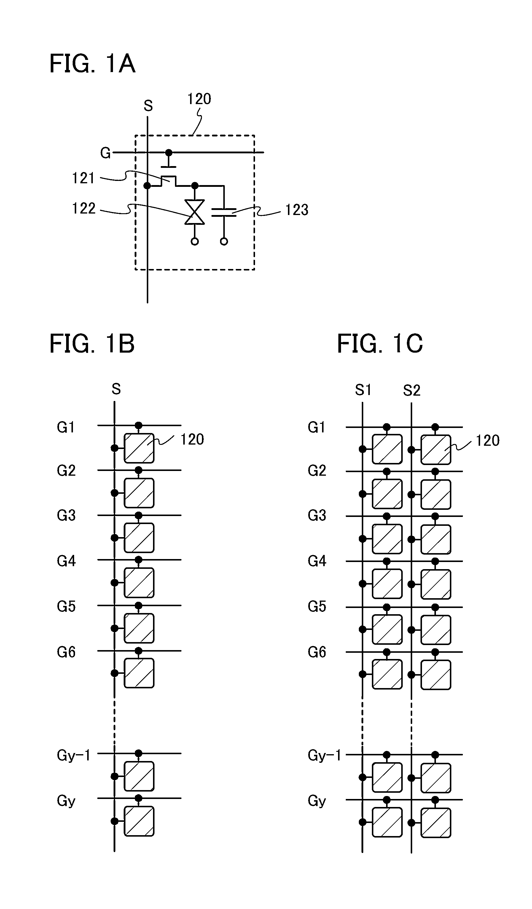
[0058]FIG. 1A shows one example of an equivalent circuit of a pixel provided in a display portion. As illustrated in FIG. 1A, the pixels 120 includes a transistor 121, a display element 122, and a capacitor 123. In addition to the transistor, the display element, and the capacitor, the pixel 120 may also include another transistor, a diode, a resistor, another capacitor, an inductor, and / or the like.

[0059]As illustrated in FIG. 1A, a gate of a transistor 121 is electrically connected to a first wiring G. One of a source and a drain of the transistor 121 is electrically connected to a s...

embodiment 2

[0091]In this embodiment, various modes of a display portion in a display device will be described.

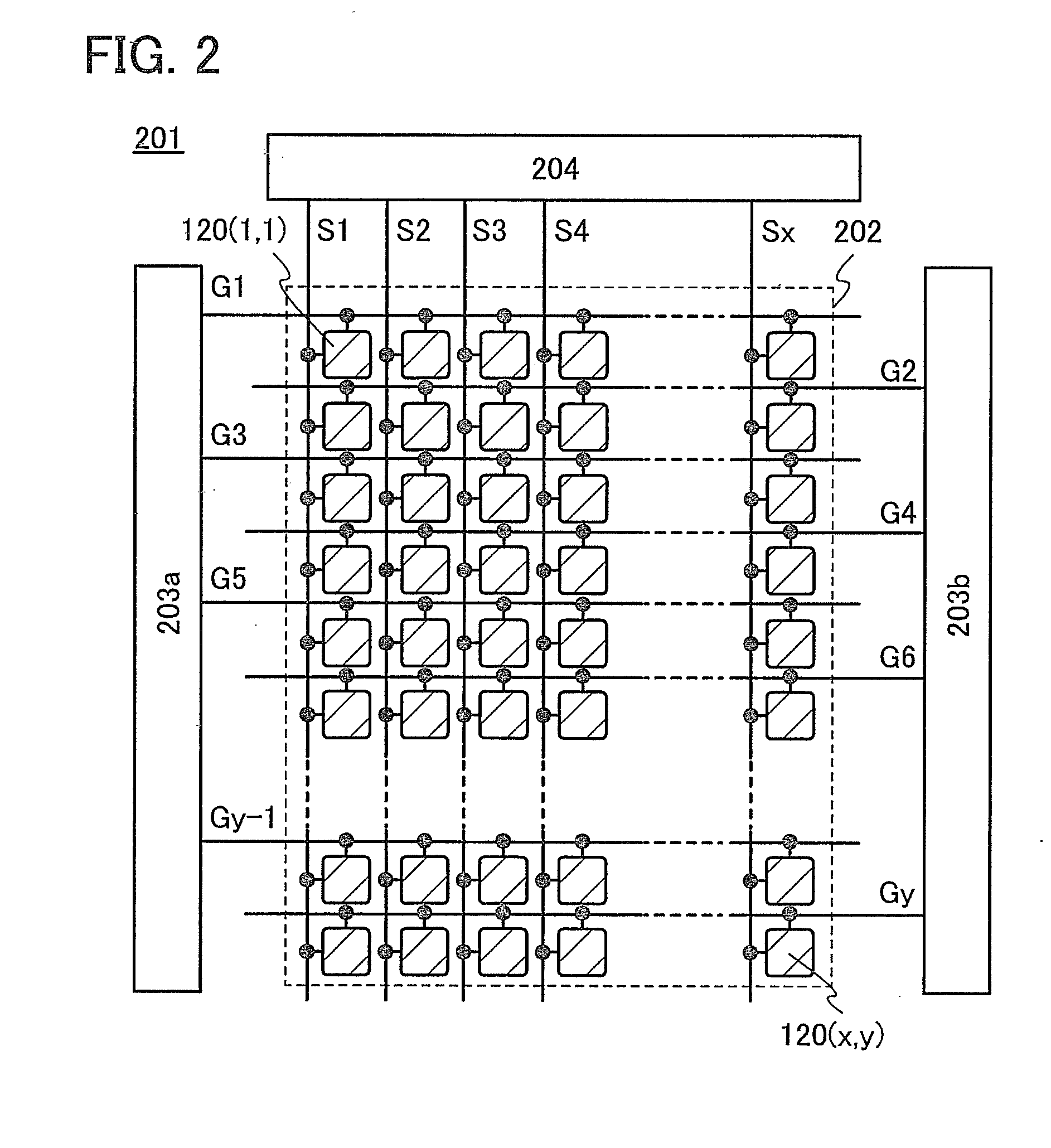
[0092]FIG. 4 illustrates one embodiment of a display portion. A display portion 211 illustrated in FIG. 4 includes the pixel portion 202, the second driver circuit 204, the control device 205, a plurality of wirings 12a to 12x, and switches 13a to 13x. Note that in FIG. 4, the first driver circuit, the plurality of first wirings G1 to Gy, and the like are omitted.

[0093]The pixel portion 202 includes the plurality of second wirings S1 to Sx and the plurality of pixels 120(1,1) to 120(x, y). In FIG. 4, the pixel portion 202 includes the x second wirings S1 to Sx and the plurality of pixels 120(1,1) to 120(x, y) provided in matrix of y pixels in column and x pixels in row.

[0094]In the display portion 211 illustrated in FIG. 4, in the plurality of second wirings S1 to Sx, the second wirings S in the odd-numbered columns are electrically connected to a wiring 11a through switches 13a, 13c ....

embodiment 3

[0113]In this embodiment, various modes of a display portion in a display device will be described.

[0114]FIG. 7 illustrates one embodiment of a pixel portion. A pixel portion 212 illustrated in FIG. 7 includes the first wirings G1 to Gy, the second wirings S1 to Sx, and the plurality of pixels 120. A difference between the pixel portion 212 and the pixel portion described in the above embodiment is a connection relation between the second wirings S1 to Sx and the plurality of pixels 120.

[0115]In the pixel portion 212 illustrated in FIG. 7, the pixels 120 in the first wirings G in the odd-numbered rows are electrically connected to the second wirings S in the odd-numbered columns, while the pixels 120 in the first wirings G in the even-numbered rows are electrically connected to the first wirings S in the even-numbered columns.

[0116]In the pixel portion 212 illustrated in FIG. 7, like that in FIG. 1C, in the plurality of pixels 120, the pixels in all of the odd-numbered rows (or even...


PUM


Abstract

To provide a novel display device where display quality does not deteriorate. The display device includes a display portion configured to display a still image at a frame frequency of 30 Hz or lower. The display portion includes a driver circuit, a plurality of wirings, and a pixel portion. The pixel portion comprises a plurality of pixels. Each of the plurality of pixels comprises a transistor, a display element, and a capacitor. A channel is formed in an oxide semiconductor layer included in the transistor. A gate of the transistor is electrically connected to one of the plurality of wirings. The driver circuit performs scanning where the plurality of wirings in one of odd-numbered rows and even-numbered rows are sequentially selected and scanning where the plurality of wirings in the other of the odd-numbered rows and the even-numbered rows are sequentially selected.

Description

BACKGROUND OF THE INVENTION[0001]1. Field of the Invention[0002]The present invention relates to an object, a method, a manufacturing method, a process, a machine, manufacture, or a composition of matter. In particular, the present invention relates to, for example, a semiconductor device, a display device, a light-emitting device, a driving method thereof, or a manufacturing method thereof. In particular, the present invention relates to a semiconductor device including an oxide semiconductor, a display device including an oxide semiconductor, or a light-emitting device including an oxide semiconductor, for example.[0003]2. Description of the Related Art[0004]The information revolution has progressed rapidly with technological innovation, mainly with innovation in information processing, and the variety of uses of displays, for example, for personal computers and mobile devices has increased at workplaces and homes. Accordingly, the frequency and time of use of displays have increa...

Claims


Application Information

Patent Timeline
Patent Type & Authority Applications(United States)
IPC IPC(8): G09G3/36
CPCG09G3/3611G02F1/13338G02F1/13454G09G3/3677G09G3/3688G09G2310/0224G09G2310/0286G09G2310/0297G09G2320/0247
Inventor MIYAKE, HIROYUKIKIMURA, HAJIMENAKAMURA, YASUONISHIDA, ERIKO
Owner SEMICON ENERGY LAB CO LTD
Why Eureka
Try Eureka