Semiconductor apparatus for fingerprint recognition

a technology of semiconductor apparatus and fingerprint recognition, applied in the field of semiconductor apparatus, can solve the problems of circuit damage and loss of function of semiconductor apparatus for fingerprint recognition

Inactive Publication Date: 2006-04-18
SONY CORP
View PDF5 Cites 19 Cited by
  • Summary
  • Abstract
  • Description
  • Claims
  • Application Information

AI Technical Summary

Benefits of technology

[0023]In this situation, the present inventor has made extensive and intensive studies with a view toward solving the above-mentioned problems accompanying the prior art. As a result, it has unexpectedly been found that the semiconductor apparatus comprising: a substrate having a transistor; a first electrode formed on the substrate and connected to the transistor; a second electrode formed on the substrate and electrically separated from the first electrode; and an insulating film formed on the substrate so as to cover the first electrode, wherein, when a plane of the insulating film which is not on a side of the substrate is taken as a first plane, a surface facing the first plane of the first electrode is taken as a first surface, and a surface facing the first plane of the second electrode is taken as a second surface, a distance between a surface of the substrate and the second surface is larger than a distance between the surface of the substrate and the first surface is free from the above-mentioned problems accompanying the prior art semiconductor apparatus. Specifically, by virtue of having the above unique structure, the semiconductor apparatus of the present invention is advantageous in that, when a finger or any other material which is electrostatically charged is brought closer to the substrate, the static electricity is not discharged into the electrode but into the static-electricity drawing wiring and then drawn out of the semiconductor apparatus, so that the semiconductor devices, the circuits and the like which are connected to the electrode can be prevented from suffering a damage due to the static electricity and from losing the functions thereof. The present invention has been completed, based on the above novel finding.
[0024]Accordingly, it is an object of the present invention to provide a semiconductor apparatus which is advantageous in that, when a finger or any other material which is electrostatically charged is brought closer to the substrate, the semiconductor devices, the circuits and the like which are connected to the electrode can be prevented from suffering a damage due to the static electricity and from losing the functions thereof.
[0025]It is another object of the present invention to provide a semiconductor apparatus for fingerprint recognition which is advantageous in that, when a finger which is electrostatically charged is brought closer to the fingerprint-recognizing surface, the semiconductor devices, the circuits and the like which are connected to the electrode can be prevented from suffering a damage due to the static electricity and from losing the functions thereof.

Problems solved by technology

However, the conventional semiconductor device for fingerprint recognition mentioned above poses a problem in that, when a finger is in contact with the fingerprint-recognizing surface, the static electricity charged in the human body is discharged in the electrodes 52 (21) and a large amount of a current flows through the electrodes 52 (21) into the detecting circuit formed on the same semiconductor substrate (see FIG. 5B), so that the circuit is damaged and the function as the semiconductor apparatus for fingerprint recognition is lost.

Method used


Image

  • Semiconductor apparatus for fingerprint recognition
  • Semiconductor apparatus for fingerprint recognition
  • Semiconductor apparatus for fingerprint recognition

Examples


first embodiment

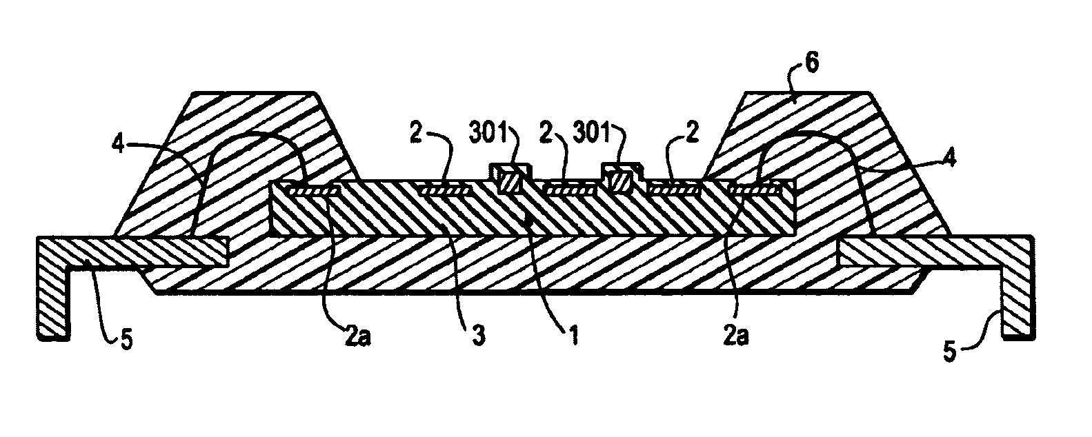
[0047]With respect to the semiconductor apparatus for fingerprint recognition which is operated as mentioned above, the present invention is described with reference to FIG. 1.

[0048]FIG. 1 is a diagrammatic cross-sectional view of a semiconductor apparatus for fingerprint recognition according to the first embodiment of the present invention, which constitutes a capacitive mode fingerprint sensor.

[0049]In the present embodiment, a wiring 301 for drawing static electricity (hereinafter, frequently referred to as “static-electricity drawing wiring 301”) having a thickness larger than that of an electrode 2 is formed along the line in the longitudinal direction of the electrode 2 (so that the lower surfaces of the wiring 301 and the electrode 2 are aligned in this example). The static-electricity drawing wiring 301 is formed electrically independently from the electrode 2.

[0050]An insulating protecting film 3, such as a passivation film, is formed so as to cover the electrodes 2, the s...

second embodiment

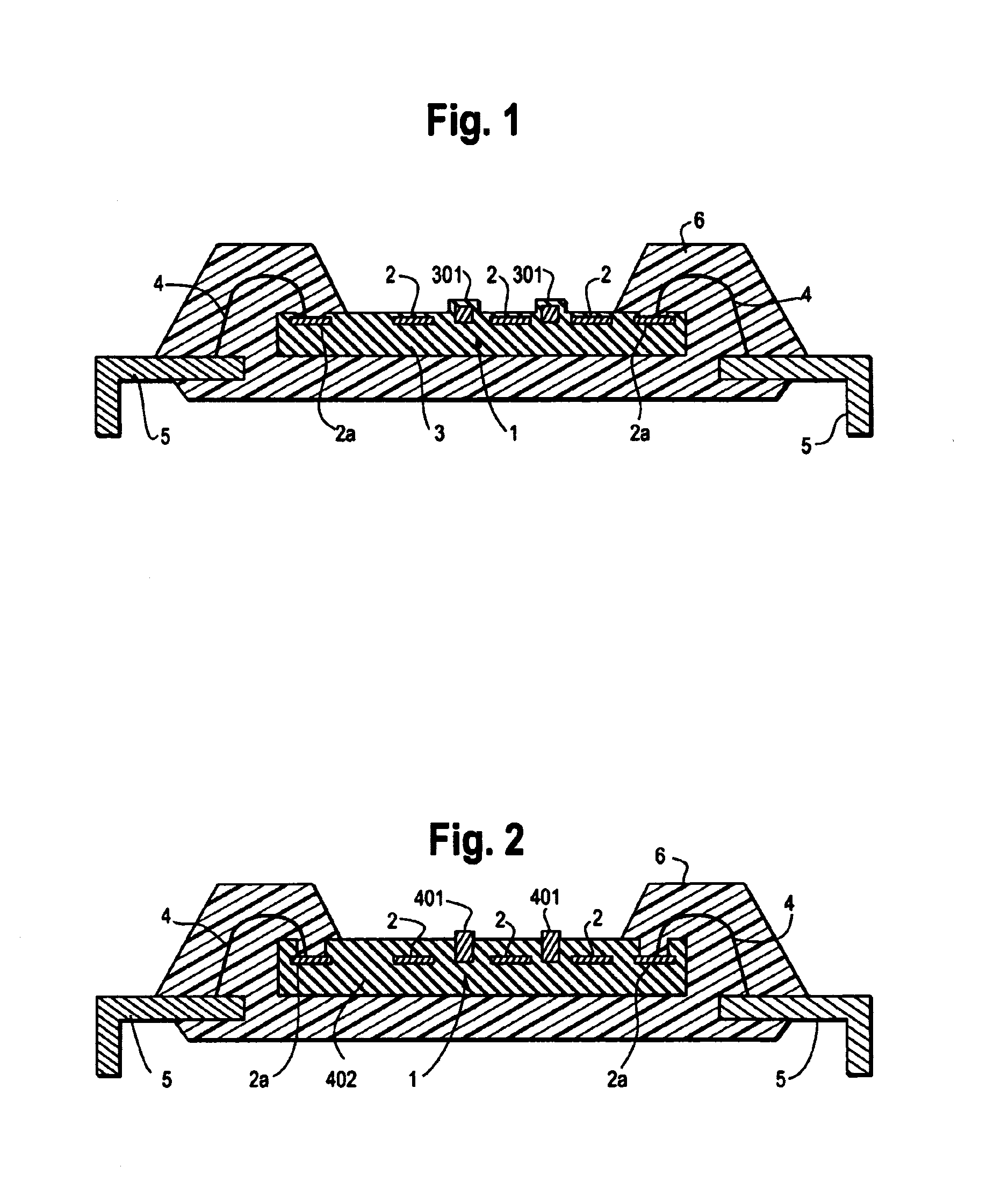
[0061]Next, the present invention is described with reference to FIG. 2.

[0062]The function as a semiconductor device for fingerprint recognition of the second embodiment is the same as that of the above-mentioned first embodiment, and therefore, only the wiring for drawing static electricity, which is a characteristic feature of the present invention, is described below.

[0063]In the present embodiment, a wiring 401 for drawing static electricity (hereinafter, frequently referred to as “static-electricity drawing wiring 401”) having a thickness larger than that of an electrode 2 is formed along the line in the longitudinal direction of the electrode 2 (so that the lower surfaces of the wire 401 and the electrode 2 are aligned in this example). The static-electricity drawing wiring 401 is formed electrically independently from the electrode 2.

[0064]An insulating protecting film 402, such as a passivation film, is formed so as to cover both of the electrode 2 and a pad electrode 2a, an...

third embodiment

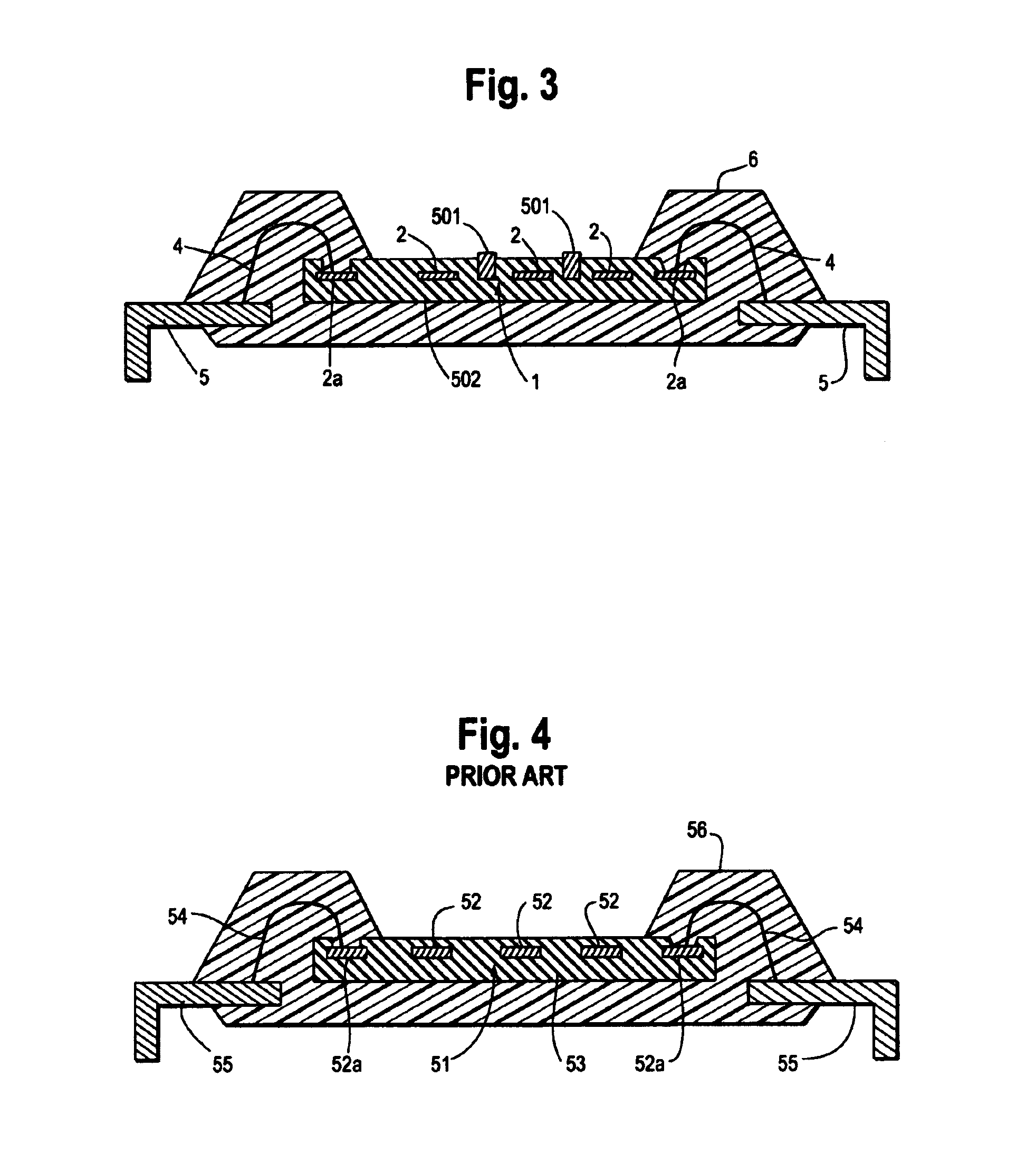
[0074]Next, the present invention is described with reference to FIG. 3.

[0075]The function as a semiconductor apparatus for fingerprint recognition of the third embodiment is the same as that of the above-mentioned first embodiment, and therefore, only the wiring for drawing static electricity, which is a characteristic feature of the present invention, is described below.

[0076]In the present embodiment, a wiring 501 for drawing static electricity (hereinafter, frequently referred to as “static-electricity drawing wiring 501”) having a thickness larger than that of an electrode 2 is formed along the line in the longitudinal direction of the electrode 2 (so that the lower surfaces of the wiring 501 and the electrode 2 are aligned in this example). The static-electricity drawing wiring 501 is formed electrically independently from the electrode 2.

[0077]An insulating protecting film 502, such as a passivation film, is formed so as to cover both of the electrode 2 and a pad electrode 2a...


PUM


Abstract

A semiconductor apparatus, which comprises: a substrate having a transistor; a first electrode formed on the substrate and connected to the transistor; a second electrode formed on the substrate and electrically separated from the first electrode; and an insulating film formed on the substrate so as to cover the first electrode, wherein, when a plane of the insulating film which is not on a side of the substrate is taken as a first plane, a surface facing the first plane of the first electrode is taken as a first surface, and a surface facing the first plane of the second electrode is taken as a second surface, a distance between a surface of the substrate and the second surface is larger than a distance between the surface of the substrate and the first surface. By virtue of having the above unique structure, the semiconductor apparatus of the present invention is advantageous in that, when a finger or any other material which is electrostatically charged is brought closer to the substrate, the static electricity is not discharged into the electrode but into the static-electricity drawing wiring and then drawn out of the semiconductor device, so that the semiconductor devices, the circuits and the like which are connected to the electrode can be prevented from suffering a damage due to the static electricity and from losing the functions thereof.

Description

RELATED APPLICATION DATA[0001]The present application claims priority to Japanese Application No. P11-323051 filed Nov. 12, 1999, which application is incorporated herein by reference to the extent permitted by law.BACKGROUND OF THE INVENTION[0002]1. Field of the Invention[0003]The present invention relates to a semiconductor apparatus. More particularly, the present invention is concerned with a semiconductor apparatus for fingerprint recognition used as a capacitive mode fingerprint sensor.[0004]2. Description of the Related Art[0005]In recent years, the fingerprint matching system, which has conventionally been utilized in the applications of the administration of entrance and exit and the like, is being attracting attention as a security system for the computer network and a personal identification tool in a portable terminal or the like. Examples of fingerprint detecting methods using the fingerprint matching system include an optical detection method, and a capacitive sensing ...

Claims


Application Information

Patent Timeline
Patent Type & Authority Patents(United States)
IPC IPC(8): G06K9/00A61B5/117G01B7/28G01B7/34H01L21/3205H01L23/52
CPCG06K9/0002H01L2224/48091H01L2224/48247H01L2924/1815H01L2224/45144H01L2924/00014H01L2924/00G06V40/1306G06F18/00
Inventor SHINOHARA, MAMORU
Owner SONY CORP
Why Eureka
Try Eureka