Piezoelectric element, ink jet head, angular velocity sensor, manufacturing method thereof, and ink jet type recording apparatus

a technology of piezoelectric elements and manufacturing methods, which is applied in the direction of piezoelectric/electrostrictive device details, device material selection, instruments, etc., can solve the problems of increasing and thus the cost of piezoelectric elements used in ink jet heads, and achieves desirable printing performance and durability, and achieves easy-to-use ink jet recording apparatuses. , the effect of good oriented film

Inactive Publication Date: 2006-04-25
PANASONIC CORP
View PDF27 Cites 16 Cited by
  • Summary
  • Abstract
  • Description
  • Claims
  • Application Information

AI Technical Summary

Benefits of technology

[0068]With the 23rd and 24th inventions, it is possible to easily obtain an ink jet recording apparatus that provides a quite desirable printing performance and durability.

Problems solved by technology

However, this method uses an MgO single crystal substrate as a base substrate, thereby increasing the cost of a piezoelectric element, and thus the cost of an ink jet head using the piezoelectric element.
Moreover, another drawback is that the variety of the substrate material is limited to the MgO single crystal.
However, while the methods described above are desirable methods that do not use an expensive MgO single-crystal substrate, it is difficult to obtain a well-oriented film having a desirable crystallinity in the film formation process, as in the case of forming a piezoelectric thin film on an MgO single-crystal substrate, because the piezoelectric thin film is formed by a sol-gel method.
Moreover, when piezoelectric elements are mass-produced with a sol-gel method, the amorphous piezoelectric precursor thin film is likely to be cracked due to changes in the volume during the degreasing step of removing organic substances.
Furthermore, in the step of heating and crystallizing the amorphous piezoelectric precursor thin film at a high temperature, the film is likely to be cracked or peeled off from the lower electrode due to crystal changes.
Therefore, as with a sol-gel method, the film is likely to be cracked or peeled off from the lower electrode due to crystal changes in the step of heating and crystallizing the film at a high temperature.
The crystallization of the PZT film proceeds gradually from the lower electrode side to the upper electrode side with a sol-gel method, whereas with a CVD method or a sputtering method, the crystallization of the PZT film proceeds randomly, resulting in irregular crystallization, and thus making the orientation control difficult.

Method used


Image

  • Piezoelectric element, ink jet head, angular velocity sensor, manufacturing method thereof, and ink jet type recording apparatus
  • Piezoelectric element, ink jet head, angular velocity sensor, manufacturing method thereof, and ink jet type recording apparatus
  • Piezoelectric element, ink jet head, angular velocity sensor, manufacturing method thereof, and ink jet type recording apparatus

Examples


embodiment 1

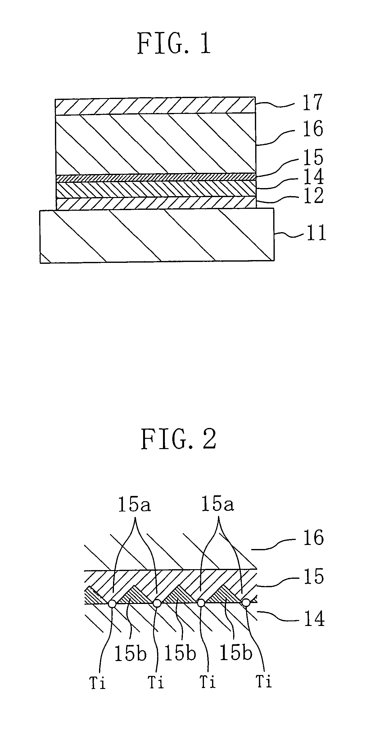
[0089]FIG. 1 illustrates a piezoelectric element according to an embodiment of the present invention. In the figure, the reference numeral 11 denotes a substrate made of a 4-inch silicon (Si) wafer having a thickness of 0.3 mm, and an adhesive layer 12 made of titanium (Ti) and having a thickness of 0.02 μm is formed on the substrate 11. Note that the substrate 11 is not limited to an Si substrate, but may alternatively be a glass substrate, a metal substrate, a ceramic substrate, or the like.

[0090]A first electrode layer 14 having a thickness of 0.22 μm and made of platinum (Pt) to which 2.1 mol % of Ti is added is formed on the adhesive layer 12. The first electrode layer 14 is oriented along the (111) plane.

[0091]An orientation control layer 15 made of PLT having a cubic or tetragonal perovskite crystalline structure whose lanthanum (La) content is 12 mol % and whose lead content is 8 mol % in excess of the stoichiometric composition is formed on the first electrode layer 14. The...

example 1

[0119]A piezoelectric element of Example 1 was produced by using the same material, thickness and manufacturing method for each film as those of the embodiment described above. No crack or peeling off was observed for any of the films of the piezoelectric element of Example 1.

[0120]The crystal orientation and the film composition of the piezoelectric layer before the formation of the second electrode layer were examined. Specifically, an analysis by an X-ray diffraction method showed that the piezoelectric layer had a (100)-oriented rhombohedral perovskite crystalline structure (degree of (100) orientation: α=97%). Moreover, an analysis of the composition of the PZT film with an X-ray microanalyzer showed that the Zr / Ti ratio was 53 / 47 as in the target composition.

[0121]Then, the crystal orientation and the film composition of the first electrode layer before the formation of the orientation control layer were examined. Specifically, an analysis by an X-ray diffraction method showed...

example 2

[0125]In Example 2, a 4-inch stainless steel (SUS304) having a thickness of 0.25 mm was used as the substrate, a tantalum (Ta) film having a thickness of 0.01 μm was used as the adhesive layer, a Pt film having a thickness of 0.25 μm and containing 8 mol % of titanium oxide was used as the first electrode layer, a PLT film (to which 3 mol % of magnesium was added) having a thickness of 0.03 μm and containing 17 mol % of lanthanum in which the lead content was 6 mol % in excess of the stoichiometric composition was used as the orientation control layer, a PZT film (Zr / Ti=40 / 60) having a thickness of 2.7 μm was used as the piezoelectric layer, and a Pt film having a thickness of 0.1 μm was used as the second electrode layer.

[0126]The adhesive layer was obtained by using a Ta target and applying a high-frequency power of 100 W thereto for 1 minute while heating the substrate to 500° C. in an argon gas at 1 Pa.

[0127]The first electrode layer was obtained by using a Ti target and a Pt ta...


PUM

PropertyMeasurementUnit
temperatureaaaaaaaaaa
thicknessaaaaaaaaaa
thicknessaaaaaaaaaa

Abstract

In a piezoelectric element, an adhesive layer 12 is provided on a substrate 11, a first electrode layer 14 made of a noble metal containing titanium or titanium oxide is provided on the adhesive layer 12, and an orientation control layer 15 that is preferentially oriented along a (100) or (001) plane is provided on the first electrode layer 14. In the vicinity of a surface of the orientation control layer 15 that is closer to the first electrode layer 14, a (100)- or (001)-oriented region extends over titanium or titanium oxide located on one surface of the first electrode layer 14 that is closer to the orientation control layer 15, and the cross-sectional area of the region in the direction perpendicular to the thickness direction gradually increases in the direction away from the first electrode layer 14 toward the opposite side. Further, a piezoelectric layer 16 that is preferentially oriented along a (001) plane is provided on the orientation control layer 15.

Description

TECHNICAL FIELD[0001]The present invention relates to a piezoelectric element having an electro-mechanical conversion function, an ink jet head using the piezoelectric element, an angular sensor, a method for manufacturing the same, and an ink jet recording apparatus including the ink jet head as printing means.BACKGROUND ART[0002]Generally, a piezoelectric material is a material capable of converting a mechanical energy to an electrical energy and vice versa. A typical example of a piezoelectric material is lead zirconate titanate having a perovskite crystalline structure (Pb(Zr,Ti)O3) (hereinafter referred to as “PZT”). In PZT, the greatest piezoelectric displacement is obtained in the <001> direction (the c axis direction) in the case of a tetragonal system, and in the <111> direction in the case of a rhombohedral system. However, many of the piezoelectric materials are polycrystals made up of a collection of crystal grains, and the crystallographic axes of the crysta...

Claims


Application Information

Patent Timeline
Patent Type & Authority Patents(United States)
IPC IPC(8): B41J2/045H01L41/04B41J2/055B41J2/135B41J2/14B41J2/16G01C19/56G01C19/5607G01C19/5621G01C19/5628H01L41/08H01L41/09H01L41/18H01L41/187H01L41/22H01L41/29H01L41/316H01L41/319H01L41/332H01L41/39
CPCB41J2/14233B41J2/161B41J2/1623B41J2/1646G01C19/5607H01L41/0815H01L41/1876H01L41/316B41J2002/14491Y10T29/49401B41J2202/03H10N30/10516H10N30/8554H10N30/076H10N30/00
Inventor FUJII, EIJITORII, HIDEOTAKAYAMA, RYOICHITOMOZAWA, ATSUSHIMURATA, AKIKOHIRASAWA, TAKU
Owner PANASONIC CORP
Why Eureka
Try Eureka