However, this type of system-level test does not ensure that the IC is
defect free, since the given applications used may exercise only a subset of the IC's functionality.
This type of high-level system-based testing also requires a relatively large amount of time.
However, given the complexity and sequential depth of modern ICs, creating a sufficiently thorough test to be applied via the pins is very difficult, and given the large number of pins on some ICs, the cost of the ATE resources can become prohibitive.
If an IC responds to such a pattern with data other than that expected, then the hypothesized fault is deduced to be present and the IC is thus determined to be defective and is not shipped.
The spectrum of all possible faults in an IC is, unfortunately, very broad.
While many defects result in permanent logical errors that can be easily detected by scan-based tests, some defects manifest themselves only as increased delays in the IC.
Therefore, if the scan test is performed without taking the speed at which the gates should respond into account, such “
delay defects” may go undetected.
For example, assuming a
NOR gate that has a weak pull down
transistor, the gate may produce the correct logical value if given enough time, but will not produce the value correctly under the timing specifications for the IC.
If the output does not change from a 1 to a 0 within specified timing margins, a slow-to-fall (STF) fault exists.
If the output does not change from a 0 to a 1 within specified timing margins, a slow-to-rise (STR) fault exists.
Due to the difficulty of making the scan enable
signal operate at speed, some designs perform transition testing at reduced speed, with consequent reduction in
test quality.
A transition fault models the situation where a single gate in an IC is slow: it will produce the correct logical output, but it will not be able to produce it in a timely fashion.
A
path delay fault models the situation where several gates are marginally slow, such that any one of them won't adversely affect the ability of the circuit to run at speed, but the combination of all the incremental delays will cause the circuit to be too slow when a path connecting those gates is sensitized.
Practical usage of the transition
fault model is impeded by the greedy nature of test generation algorithms, which tend to select the easiest (i.e., the shortest)
route into and out of the gate in question, even when there are other (longer) routes that would make the transition test more sensitive to a given
delay defect.
Practical usage of the path delay
fault model is impeded by the exponential number of paths in a circuit: testing all possible paths in an IC is a mathematical impossibility.
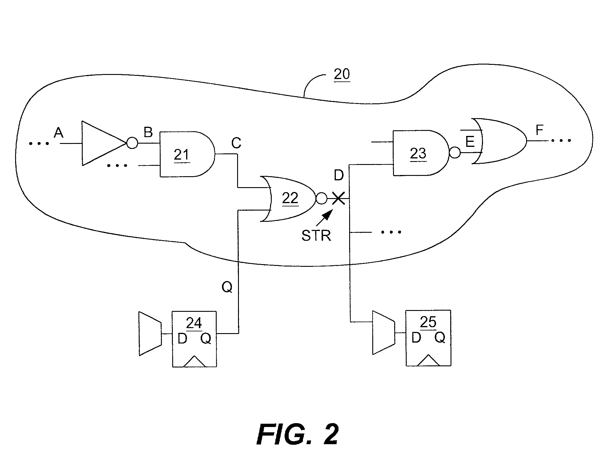
This choice, unfortunately, reduces the quality of the transition test pattern, since the length of the path through the fault site is not taken into account in determining whether or not a transition fault is detected by a test pattern.
The problem with this determination is that a delay defect at this fault site could indeed exist but the delay is just too short in duration to affect the particular (short) path Q-D taken to test it.
Clearly, the transition
fault model does not take into account whether a delay defect will cause an IC to fail when the defect is part of a longer path than that taken to test the transition fault at the defect site.
However, the application of the path delay fault model to an entire circuit results in an exponential explosion in the number of paths, rendering this model useless as a general technique for quantifying delay
fault coverage.
This results in (optimal) tests for the critical path subset of all
chip paths, but does not provide global coverage of delay defects.
Furthermore, a set of nodes on a path that is functionally unsensitizable may remain untested, even though these nodes could have been tested via another shorter, but truly, sensitizable path.

