Method of manufacturing metal gate MOSFET with strained channel

a technology of metal gate mosfet and strained channel, which is applied in the direction of semiconductor devices, electrical equipment, basic electric elements, etc., can solve problems such as affecting the mobility of the fin structur

Active Publication Date: 2006-05-09
ADVANCED MICRO DEVICES INC
View PDF4 Cites 16 Cited by
  • Summary
  • Abstract
  • Description
  • Claims
  • Application Information

AI Technical Summary

Benefits of technology

[0007]One aspect of the invention is directed to a method of manufacturing a semiconductor device. The method includes forming a fin structure on an insulator, forming a dummy gate structure over at least a portion of the fin structure and a portion of the insulator, and forming sidewall spacers adjacent first and second sides of the dummy gate structure. The method further includes removing the dummy gate structure to create a space previously occupied by the dummy gate structure and depositing a metal layer at a high temperature in the space. The metal layer forms a gate for the semiconductor device. Cooling of the metal layer after deposition of the metal layer induces strain to the fin structure.

Problems solved by technology

Cooling of the metal layer induces strain to the fin structure that affects the mobility of the fin structure.

Method used


Image

  • Method of manufacturing metal gate MOSFET with strained channel
  • Method of manufacturing metal gate MOSFET with strained channel
  • Method of manufacturing metal gate MOSFET with strained channel

Examples


Embodiment Construction

[0023]The following detailed description of the invention refers to the accompanying drawings. The same reference numbers may be used in different drawings to identify the same or similar elements. Also, the following detailed description does not limit the invention. Instead, the scope of the invention is defined by the appended claims and their equivalents.

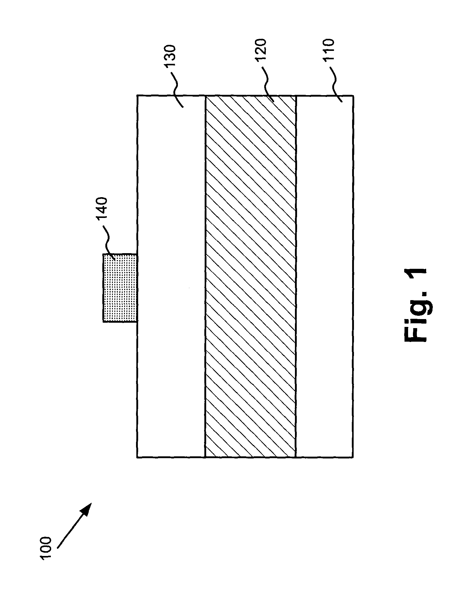
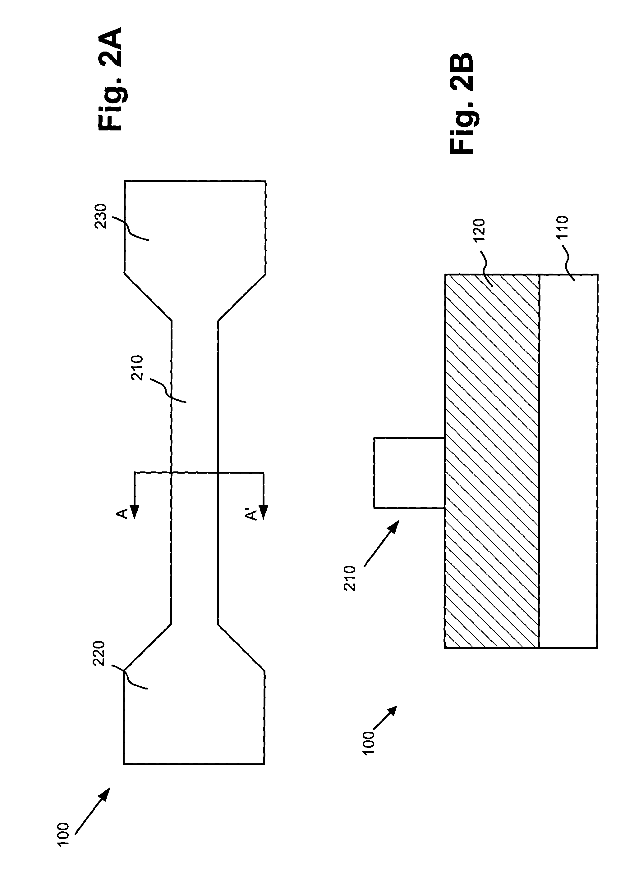
[0024]A FinFET, as the term is used herein, refers to a type of MOSFET in which a conducting channel is formed in a vertical silicon (Si) “fin.” FinFETs are generally known in the art.

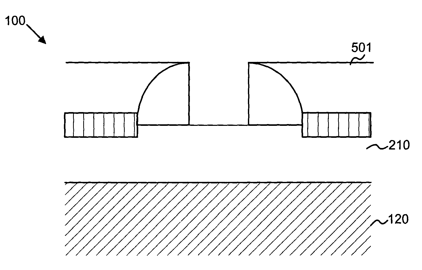
[0025]Implementations consistent with the present invention provide FinFET devices and methods of manufacturing such devices. The gates in the FinFET devices formed in accordance with the present invention may include a metal. The metal gate may be deposited and polished at high temperatures (e.g., 600°–700° C.). The subsequent cooling of the high temperature metal gate induces strain into the fin structure, leading to enhanced mobility.

[0026]FIG. ...


PUM


Abstract

A method of manufacturing a MOSFET type semiconductor device includes forming a fin structure and a dummy gate structure over the fin structure. Sidewall spacers may be formed adjacent the dummy gate structure. The dummy gate structure may be later removed and replaced with a metal layer that is formed at a high temperature (e.g., 600°–700° C.). The cooling of the metal layer induces strain to the fin structure that affects the mobility of the double-gate MOSFET.

Description

TECHNICAL FIELD[0001]The present invention relates to semiconductor devices and methods of manufacturing semiconductor devices. The present invention has particular applicability to double-gate devices.BACKGROUND ART[0002]The escalating demands for high density and performance associated with ultra large scale integration semiconductor devices require design features, such as gate lengths, below 100 nanometers (nm), high reliability and increased manufacturing throughput. The reduction of design features below 100 nm challenges the limitations of conventional methodology.[0003]For example, when the gate length of conventional planar metal oxide semiconductor field effect transistors (MOSFETs) is scaled below 100 nm, problems associated with short channel effects, such as excessive leakage between the source and drain, become increasingly difficult to overcome. In addition, mobility degradation and a number of process issues also make it difficult to scale conventional MOSFETs to inc...

Claims


Application Information

Patent Timeline
Patent Type & Authority Patents(United States)
IPC IPC(8): H01L21/311
CPCH01L29/66545H01L29/785H01L29/7842H01L29/66795H01L29/4908
Inventor YU, BINWANG, HAIHONG
Owner ADVANCED MICRO DEVICES INC
Why Eureka
Try Eureka