Defective pixel compensation system and display device using the system

a compensation system and pixel technology, applied in television systems, instruments, pulse techniques, etc., can solve problems such as deteriorating the quality of displayed images, and achieve the effects of reducing the perceptibility of defective pixels, reducing the brightness of adjacent pixels, and minimizing image deterioration

Inactive Publication Date: 2006-05-30
SEMICON ENERGY LAB CO LTD
View PDF15 Cites 6 Cited by
  • Summary
  • Abstract
  • Description
  • Claims
  • Application Information

AI Technical Summary

Benefits of technology

[0012]In view of the above-described problem, an object of the present invention is to provide a display device capable of limiting deterioration of a displayed image even in a case where a display panel having some defective pixels is used.
[0014]As a result of this data correction, the perceptibility of the defect in the image displayed by using the display panel having the defective pixel is reduced, thereby minimizing deterioration of the image.
[0020]According to the present invention, as shown in FIG. 1, brightness correction is performed with respect to the pixels in the display panel displaying the red image and the display panel displaying the blue image which have the same coordinates (m, n) as the defective pixel in the display panel displaying the green image (more specifically, correction of increasing the average brightness of the pixels 102 and 103). The human sense of sight is higher in lightness sensitivity than in chromaticity sensitivity. Therefore, by only increasing the brightness of the pixels having the same coordinates as the defective pixel, the defective pixel in the resulting image obtained by combining the images of the three display panels becomes harder to percept. In this manner, deterioration of the image can be minimized as much as possible.
[0027]means for increasing the brightness of pixels having the same coordinates as the coordinates of the defective pixel in the display panels other than the one display panel having the defective pixel out of the three display panels.
[0028]Further, as shown in FIG. 3, the other aspect of the present invention disclosed in this application is characterized in that compensation is carried out to increase brightness of pixels adjacent to the defect pixel of the green display panel in addition to the above structure. While increasing the brightness of the pixel having the same coordinates as the defect pixel, compensation is conducted for increasing the brightness of the adjacent pixels. As the result, the defect pixel in the combined image of images of the three display panels are not remarkable and it is possible to prevent as much as possible the deterioration of the image.
[0044]That is, in a direct-view type display device using one display panel, data correction is performed by increasing the brightness of pixels adjacent to the defective pixel in the display panel. This correction, based on increasing the brightness of the adjacent pixels, reduces the perceptibility of the defective pixel in the image of the display panel, thereby minimizing deterioration of the image. This correction is particularly effective in a case where the pixel size is extremely small.

Problems solved by technology

Therefore, image in this defective portion is perceptible, thus causes deteriorating the quality of the displayed image.

Method used


Image

  • Defective pixel compensation system and display device using the system
  • Defective pixel compensation system and display device using the system
  • Defective pixel compensation system and display device using the system

Examples


embodiment 1

[Embodiment 1]

[0092]In this embodiment, a rear projector is provided as an example of a projection display device of the present invention. FIG. 7 is a perspective view of the rear projector of this embodiment, showing a rear projector body 401, a projection display device 402 of the present invention, a reflector 403, and a screen 404.

[0093]The projection display device 402 uses three liquid crystal panels, and has a light source (a white light source in this embodiment), dichroic mirrors each of which reflects only light having wavelengths in a certain wavelength region and allows light having wavelengths in the other regions to pass therethrough, total reflection mirrors, etc.

[0094]In this embodiment, liquid crystal panels having digital drivers are provided. The liquid crystal panels have pixel regions for displaying red (R), green (G), and blue (B) images, source drivers, gate drivers, a digital video data division circuit, etc. The three liquid crystal display panels are all m...

embodiment 2

[Embodiment 2]

[0100]A three-plate type projector structured differently from that in the first embodiment is described in the present embodiment.

[0101]In FIG. 10, the reference numeral 701 denotes a light source, 702 and 703 denote dichroic mirrors, 704 to 706 denote total reflection mirrors, 707 to 709 denote liquid crystal panels, 710 denotes a dichroic prism and 711 denotes projection lens.

[0102]An example in which the display device according to the present embodiment is used for a front projector will be shown in FIG. 11. The reference numeral 801 denotes a main body, and 802 denotes a screen.

embodiment 3

[Embodiment 3]

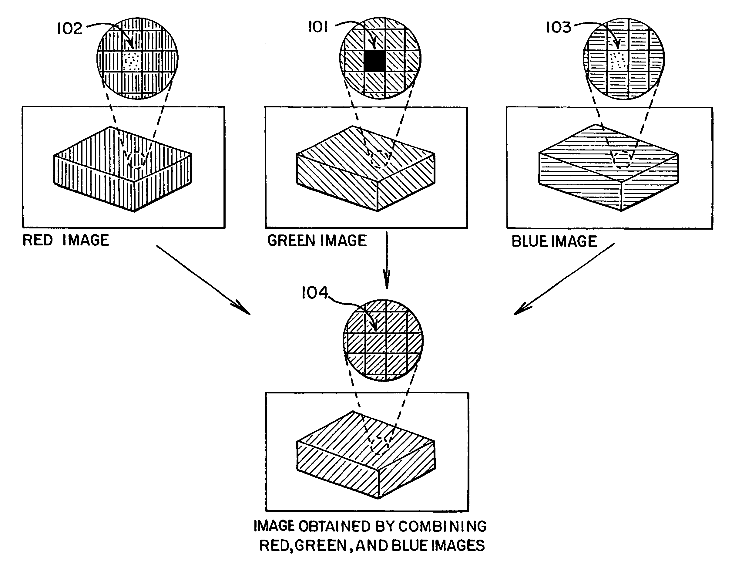
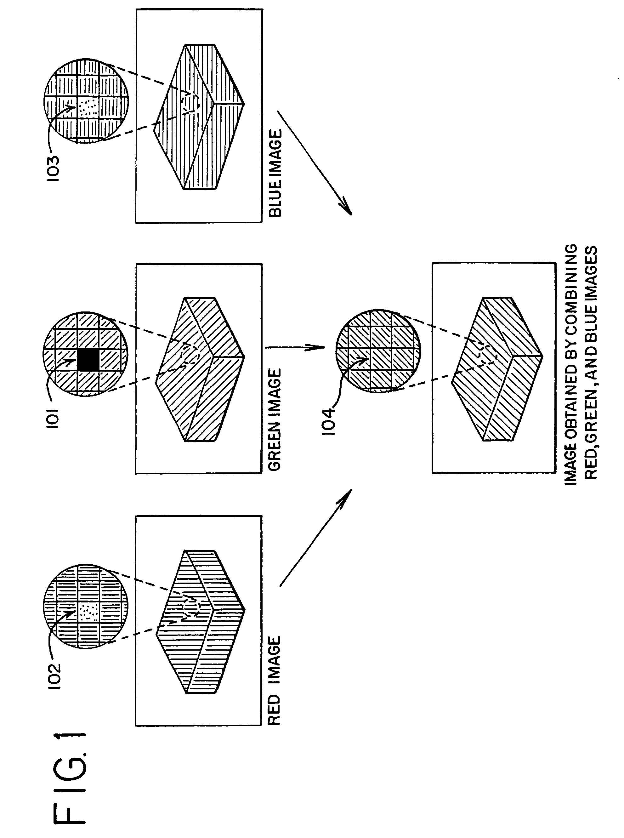
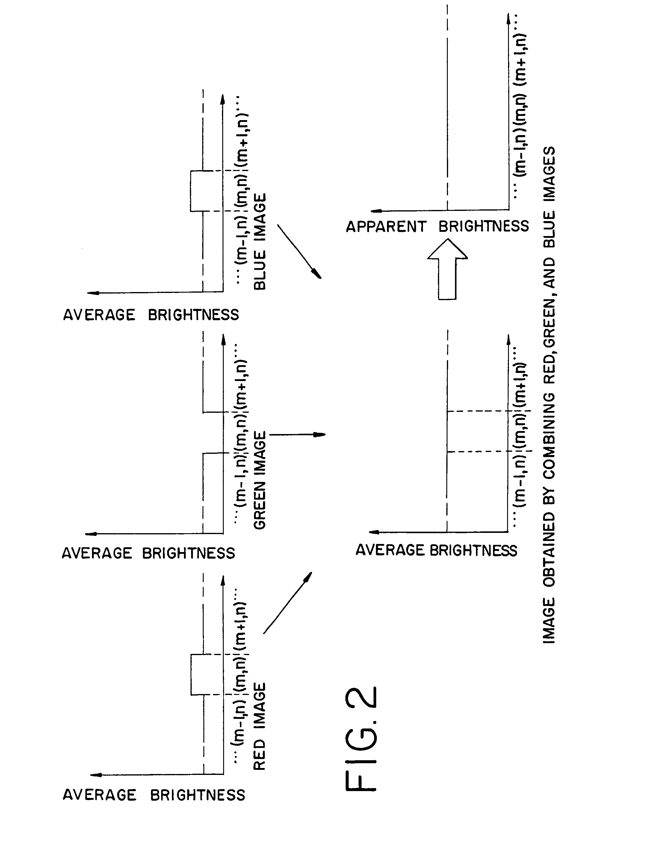
[0103]In this embodiment, the defective pixel compensation system of the present invention is operated differently from that in the first embodiment, as shown in the flowchart of FIG. 12. The process of operating the system will be described with respect to a case where the system is adapted to a display device having three liquid crystal panels already mounted therein.

[0104]First, the display device is made to operate and is confirmed whether there is any defective pixel in a color image projected onto the screen. If no defective pixel exists, the process ends and the display device is put to ordinary use. If a defective pixel exists, the coordinates of the defective pixel are determined and it is determined which panel of the red, green, and blue display panels is corresponding to the liquid crystal panel having the defective pixel.

[0105]If the liquid crystal panel with the defective pixel is the red liquid crystal panel, it is confirmed as to whether the defective p...


PUM

PropertyMeasurementUnit
transmittanceaaaaaaaaaa
glass strain temperatureaaaaaaaaaa

Abstract

With respect to a display device having a high-resolution display panel, It makes possible to prevent to deteriorate the display quality by a dot defect. A display panel having a dot defect is identified and coordinates of the defective pixel are determined. The brightnesses of pixels adjacent to the defective pixel and / or the brightnesses of pixels of other display panels having the corresponding coordinates as the dot defect are increased to reduce the apparent perceptibility of the dot defect.

Description

[0001]This application is a continuation of U.S. application Ser. No. 09 / 713,101, filed on Nov. 15, 2000 now U.S. Pat. No. 6,618,115.BACKGROUND OF THE INVENTION[0002]1. Field of the Invention[0003]The present invention relates generally to projection display devices, and more particularly, to an active matrix type projection display device, typically a rear projection type or a front projection type liquid crystal display device.[0004]2. Description of the Related Art[0005]The development of techniques for manufacturing semiconductor devices, such as a thin-film transistor (TFT), having a semiconductor thin film formed on a low-priced glass substrate, has recently been promoted with the increase in demand for active matrix liquid crystal display devices (liquid crystal panels).[0006]Also, projection type liquid crystal display devices (liquid crystal projectors) have attracted attention, in which pixel portions of liquid crystal panels are irradiated with strong light from a light s...

Claims


Application Information

Patent Timeline
Patent Type & Authority Patents(United States)
IPC IPC(8): G02F1/1335G02F1/13G09G3/00G09G3/36H04N9/31
CPCG09G3/002G09G3/3648H04N9/3197H04N9/3179H04N9/3182H04N9/3194G09G2320/0626G09G2330/08G09G2330/10
Inventor HIROKI, MASAAKI
Owner SEMICON ENERGY LAB CO LTD
Why Eureka
Try Eureka