Thin film magnetic memory device conducting read operation by a self-reference method
a magnetic memory and self-reference technology, applied in semiconductor devices, digital storage, instruments, etc., can solve the problems of reducing the manufacturing yield, increasing the manufacturing cost, and difficulty in accurately setting the reference current produced by the reference cell, so as to achieve high speed and simplify the circuit structure. , the effect of high speed
- Summary
- Abstract
- Description
- Claims
- Application Information
AI Technical Summary
Benefits of technology
Problems solved by technology
Method used
Image

Examples
first embodiment
[0057
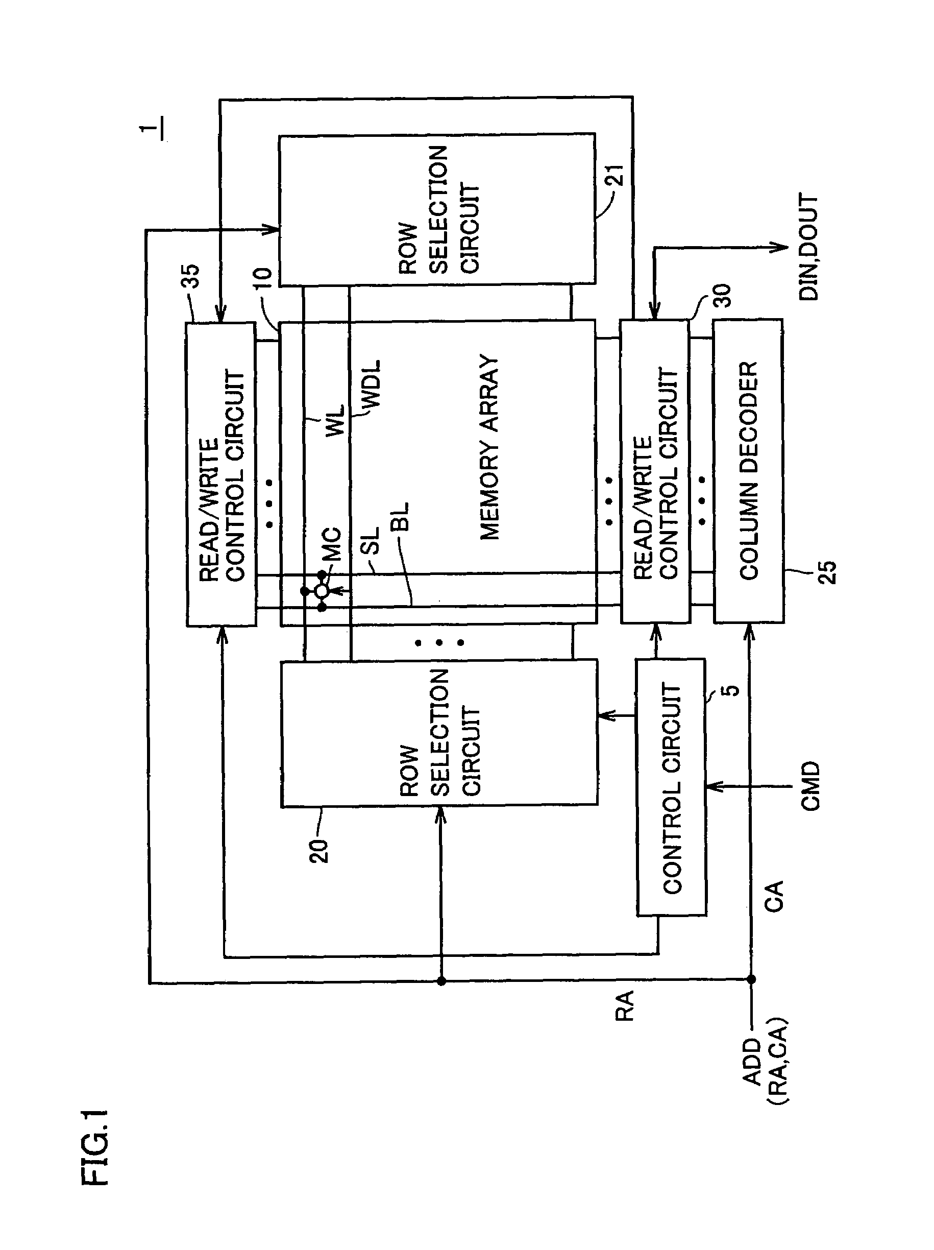
[0058]Referring to FIG. 1, an MRAM device 1 according to an embodiment of the present invention conducts random access in response to an external control signal CMD and an external address signal ADD to write input data DIN to, or read output data DOUT from, a memory cell selected for write or read operation (hereinafter, sometimes referred to as “selected memory cell”).
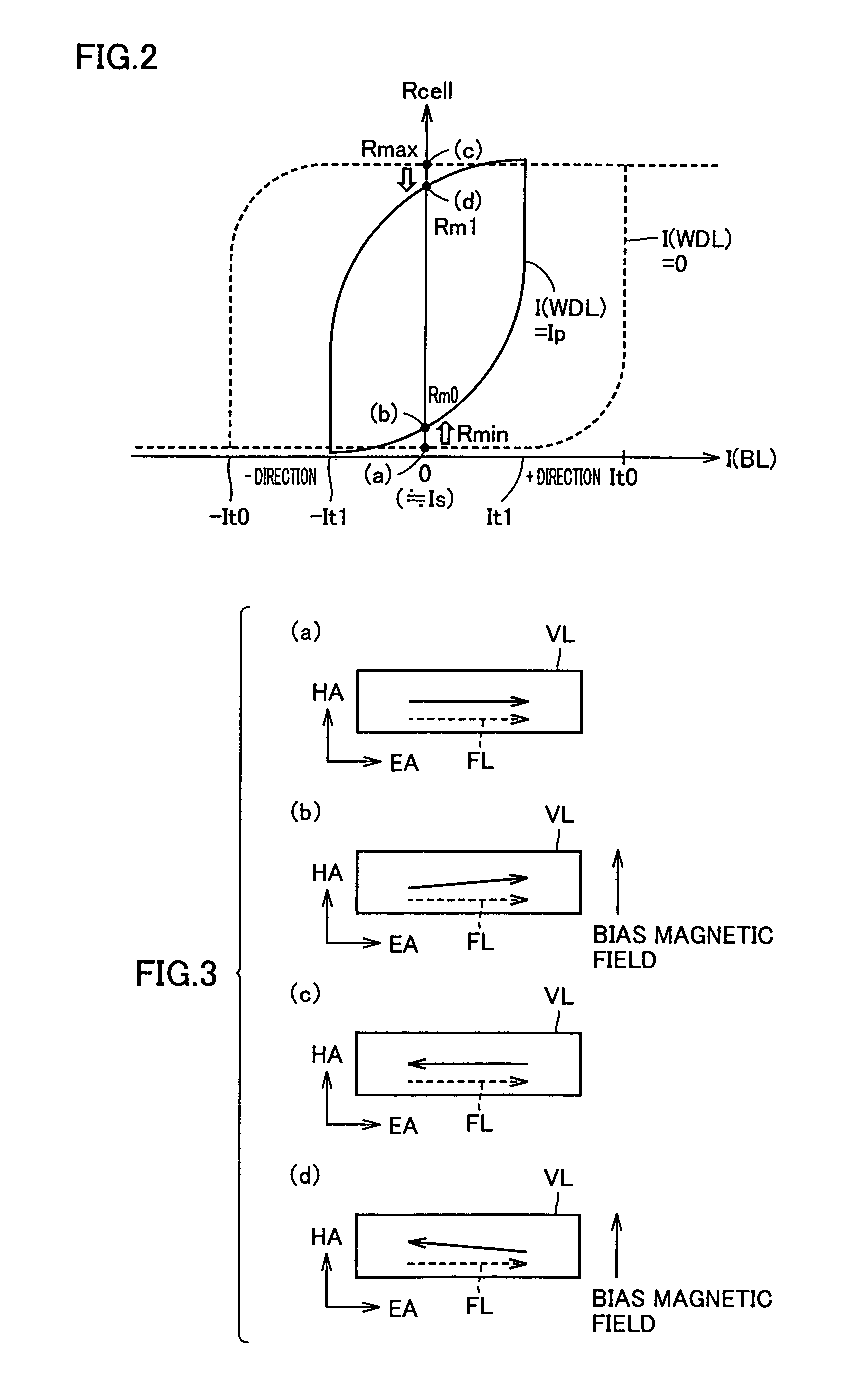
[0059]MRAM device 1 includes a control circuit 5 for controlling the overall operation of MRAM device 1 in response to control signal CMD, and a memory array 10 having MTJ memory cells MC arranged in a matrix. The structure of each MTJ memory cell and the principles of data storage of each MTJ memory cell are the same as those described in FIGS. 11 to 14.
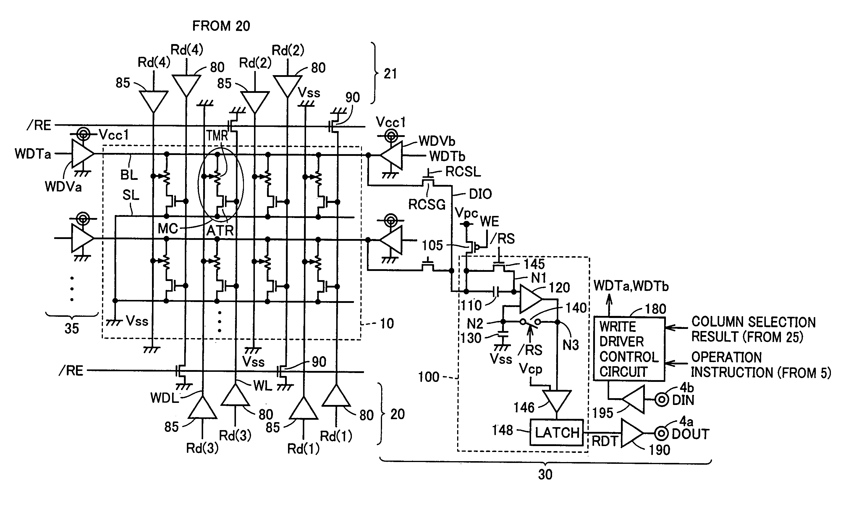
[0060]In memory array 10, word lines WL and write digit lines WDL are provided corresponding to the MTJ memory cell rows, and bit lines BL and source lines SL are provided corresponding to the MTJ memory cell columns. FIG. 1 exemplarily shows a single MTJ memory...
second embodiment
[0145
[0146]In the second embodiment, the structure for supplying a current to write digit line WDL will be described. This structure is used for both a data write current (write operation) and a bias current (read operation).
[0147]FIG. 8 is a circuit diagram showing the structure of a circuit group for controlling current supply to write digit line WDL according to the second embodiment.
[0148]Referring to FIG. 8, a write digit line driver 85 is provided for each write digit line WDL. Each write digit line driver 85 has a driver transistor 86. Driver transistor 86 is a N-channel MOS transistor, and is connected in series with a corresponding write digit line WDL between a power supply voltage line VPL for transmitting power supply voltage Vcc1 and a ground voltage line GPL. Ground voltage line GPL is connected to fixed voltage Vss through a transistor switch 88. Transistor switch 88 is turned ON / OFF in response to a control signal ACT. Control signal ACT is activated to H level durin...
PUM
 Abstract
Description
Claims
Application Information
 - R&D Engineer
- R&D Manager
- IP Professional
- Industry Leading Data Capabilities
- Powerful AI technology
- Patent DNA Extraction
Browse by: Latest US Patents, China's latest patents, Technical Efficacy Thesaurus, Application Domain, Technology Topic.
© 2024 PatSnap. All rights reserved.Legal|Privacy policy|Modern Slavery Act Transparency Statement|Sitemap