Microcontroller with multiple function blocks and clock signal control
- Summary
- Abstract
- Description
- Claims
- Application Information
AI Technical Summary
Problems solved by technology
Method used
Image

Examples
first embodiment
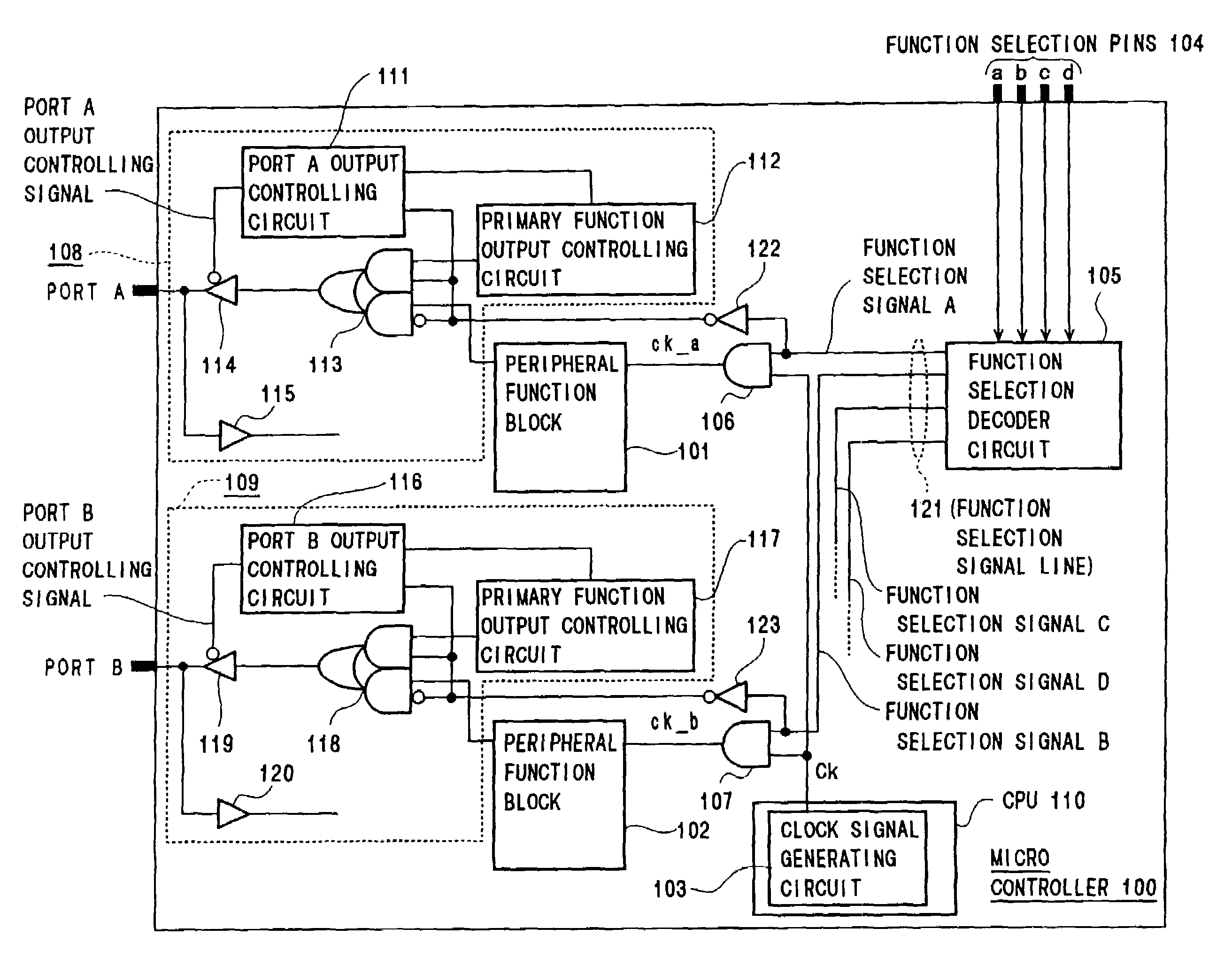
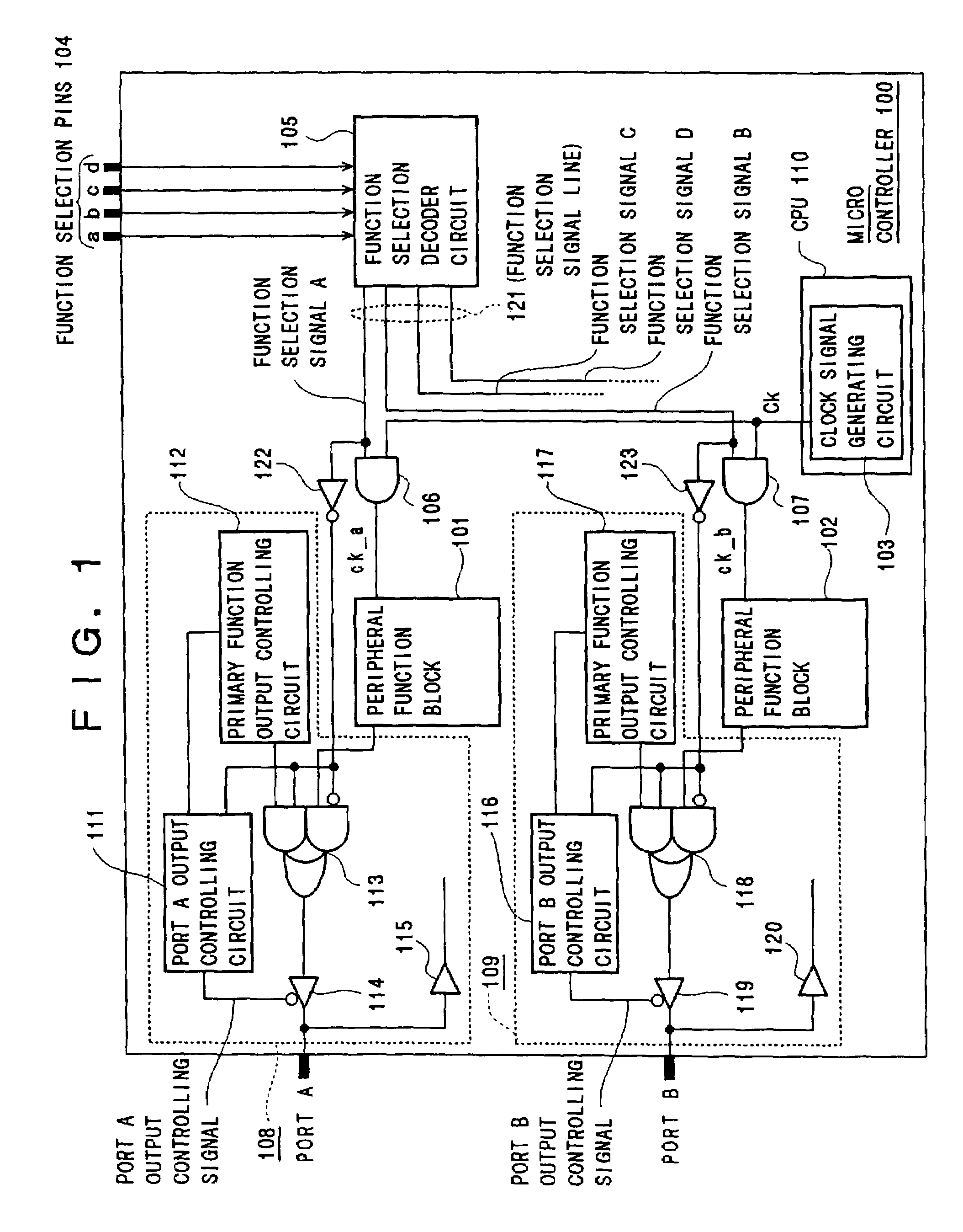
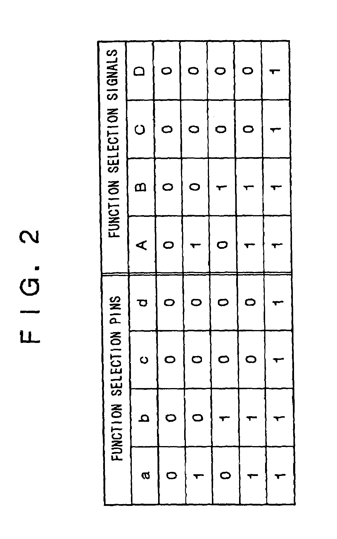
[0011]FIG. 1 is a circuit block diagram showing a configuration of a microcontroller according to a first embodiment of the present invention. The microcontroller 100 according to this embodiment includes: input / output ports (ports A and B); functional blocks (peripheral functional blocks 101 and 102), each associated with one of the ports A and B, for performing predetermined functions; a clock signal generating section (a clock signal generating circuit 103) which generates a clock signal Ck to be supplied to the peripheral functional blocks 101 and 102; function selection pins 104 (also referred to as “mode pins”) to which an external signal is input; a decoding section (a function selection decoder circuit 105) which decodes the external signal (mode signal) input via the function selection pins 104; clock signal controlling sections 106 and 107 which selectively supply the clock signal from the clock signal generating circuit 103 to the peripheral functional blocks 101 or 102 i...
second embodiment
[0024]A microcontroller according to a second embodiment of the invention will now be described. FIG. 3 is a circuit block diagram showing a configuration of the microcontroller according to the second embodiment of the invention. In addition to the elements of the microcontroller of the first embodiment shown in FIG. 1, the microcontroller of this embodiment further includes a default slave block 301, which outputs a response signal in place of the peripheral functional blocks when they are accessed from the CPU while the clock signal is not supplied thereto. The default slave block 301 has a function to output a response signal RESP and a bus-ready signal READY in place of the peripheral functional blocks when they are accessed while the clock signal is not supplied thereto.
[0025]Now, referring to FIG. 4, the default slave block 301 is described in detail. FIG. 4 is a circuit block diagram showing a configuration of the default slave block 301. The default slave block 301 includes...
PUM
 Abstract
Description
Claims
Application Information
 - Generate Ideas
- Intellectual Property
- Life Sciences
- Materials
- Tech Scout
- Unparalleled Data Quality
- Higher Quality Content
- 60% Fewer Hallucinations
Browse by: Latest US Patents, China's latest patents, Technical Efficacy Thesaurus, Application Domain, Technology Topic, Popular Technical Reports.
© 2025 PatSnap. All rights reserved.Legal|Privacy policy|Modern Slavery Act Transparency Statement|Sitemap|About US| Contact US: help@patsnap.com