Electronic and optoelectronic devices and methods for preparing same

a technology of optoelectronic devices and optoelectronic devices, applied in the direction of photometry using electric radiation detectors, optical radiation measurement, instruments, etc., can solve the problems of unsolved, and achieve the effect of facilitating the response to optical illumination

Inactive Publication Date: 2006-06-13
THE TRUSTEES OF THE UNIV OF PENNSYLVANIA
View PDF12 Cites 51 Cited by
  • Summary
  • Abstract
  • Description
  • Claims
  • Application Information

AI Technical Summary

Problems solved by technology

The advantages afforded by such devices are already established theoretically, and it remains a challenge to create such devices with the beneficial properties predicted.
A formidable technical problem which remains unsolved is to devise a way to successfully position various different elements in a directed manner so as to produce devices, connect them to other components, such as electrodes, and integrate them into conventional as well as news systems (e.g., plasmonic systems).

Method used


Image

  • Electronic and optoelectronic devices and methods for preparing same
  • Electronic and optoelectronic devices and methods for preparing same
  • Electronic and optoelectronic devices and methods for preparing same

Examples


examples

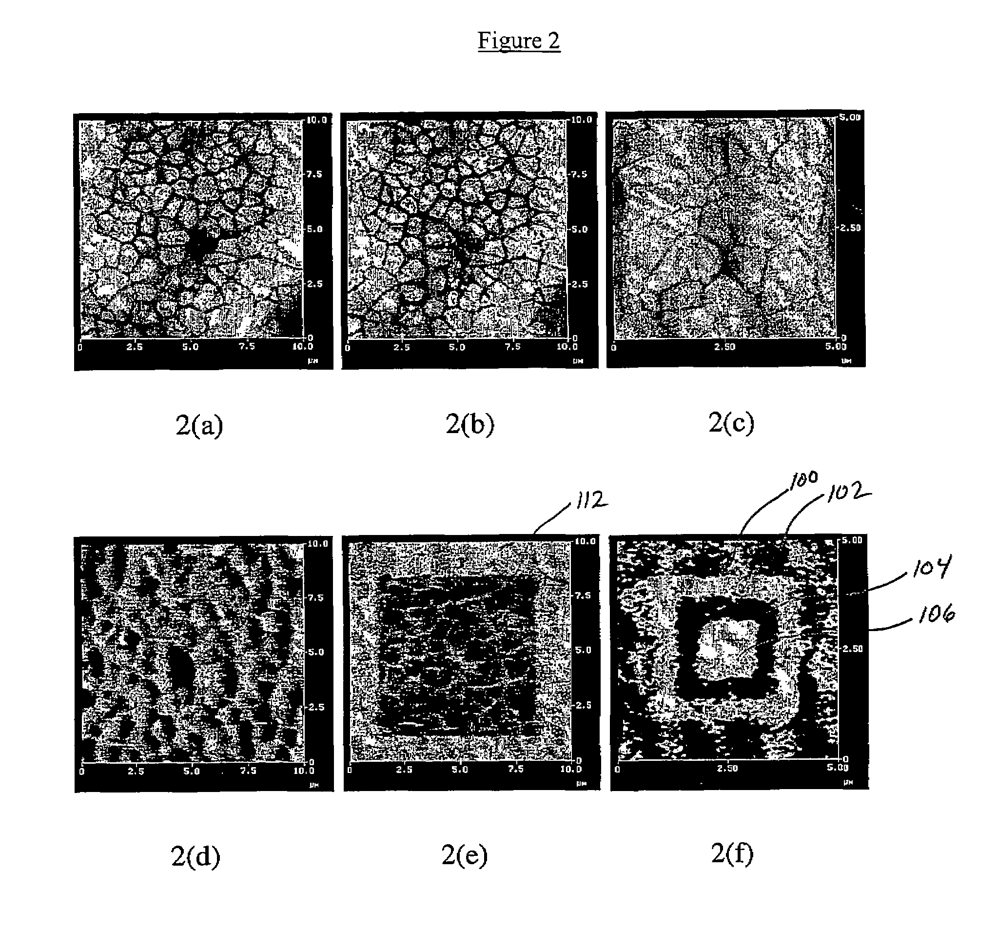
[0080]FIG. 2 is an illustrative example of a lead zirconate titanate substrate patterned in accordance with step 1(a) of FIG. 1. Prior to writing the substrate to orient the domains, contact-mode AFM and piezoresponse force microscopy (PFM) measurements were performed using a commercial instrument (Digital Instruments Dimension 3000 NS-III) to characterize the topography, FIG. 2(a), and polarization distribution, FIG. 2(d), of the surface. To perform piezoresponse measurements, the AFM was additionally equipped with a function generator and lock-in amplifier (DS340, SRS 830, Stanford Research Systems). Platinum coated tips (1>>125 μm, resonant frequency about 350 kHz, SiliconMDT NSCS12 Pt) were used for these measurements. After characterization of the initial state of the substrate surface, selected portions of the surface were addressed to provide regions of switched polarization.

[0081]The tip of the AFM was biased −10 Vdc and scanned over a square region of the substrate surface ...


PUM

PropertyMeasurementUnit
distanceaaaaaaaaaa
voltage biasaaaaaaaaaa

Abstract

Disclosed are electronic, plasmonic and opto-electronic components that are prepared using patterned photodeposited nanoparticles on a substrate surface. Also disclosed are ferroelectric nanolithography methods for preparing components, circuits and devices.

Description

CROSS REFERENCE TO RELATED APPLICATIONS[0001]This application is a continuation-in-part of U.S. application Ser. No. 10 / 344,810, filed Sep. 3, 2003 now U.S. Pat. No. 6,982,174, which is a PCT National Phase application of PCT / US01 / 41726, filed Aug. 15, 2001, which claims the benefit of U.S. Provisional Application No. 60 / 225,261, filed Aug. 15, 2000. This application also claims the benefit of U.S. Provisional Application No. 60 / 667,539, filed Apr. 1, 2005. Each of the aforementioned applications are incorporated by reference herein in their entirety.STATEMENT OF GOVERNMENT RIGHTS[0002]The invention was made with U.S. Government support. The Government may have certain rights in the invention through the National Science Foundation under federal grant number NSF DMR03-04531.FIELD OF THE INVENTION[0003]The present invention pertains to electronic and opto-electronic devices and their fabrication. The present invention also pertains to ferroelectric nanolithography methods.BACKGROUND ...

Claims


Application Information

Patent Timeline
Patent Type & Authority Patents(United States)
IPC IPC(8): H01L21/00H01L21/203G01J1/42G01Q70/14H01L31/08H01L31/18H01L51/42
CPCB81B1/00B82B3/00B82Y10/00B82Y30/00B82Y40/00H01L31/08H01L31/18H01L51/0595B82Y20/00H01L51/428G01J1/42G01Q80/00G01J1/0204H10K10/701H10K30/65
Inventor BONNELL, DAWN A.LEI, XIAOJUNCONKLIN, DAVID JOSEPH
Owner THE TRUSTEES OF THE UNIV OF PENNSYLVANIA
Why Eureka
Try Eureka