Semiconductor manufacturing apparatus, management apparatus therefor, component management apparatus therefor, and semiconductor wafer storage vessel transport apparatus

a semiconductor wafer storage vessel and management apparatus technology, applied in the direction of electrical programme control, instruments, program control, etc., can solve the problems of requiring a long time and much labor of the repairer, affecting the service life of the faulty portion, and affecting the product manufacturing process

Inactive Publication Date: 2006-06-20
KK TOSHIBA
View PDF6 Cites 14 Cited by
  • Summary
  • Abstract
  • Description
  • Claims
  • Application Information

AI Technical Summary

Benefits of technology

[0032]According to one aspect of the present invention, a semiconductor wafer storage vessel transport apparatus having a transport vehicle which transports a semiconductor wafer storage vessel and a control device which controls operation of the transport vehicle comprises a storage device which stores, for each of portions in the transport vehicle and the control device, information representing a lapsed time of use till occurrence of a failure after start of use, a transport count, or a moving distance, and a calculation device which receives the information stored in the storage device, and outputs function information representing a failure probability and / or a failure rate as a function of the lapsed time of use, the transport count, or the moving distance for each portion.

Problems solved by technology

If a failure occurs in a semiconductor manufacturing apparatus and production cannot continue on a semiconductor device manufacturing line, the manufacture of a product during production by the apparatus stops, resulting in a product manufacturing delay or a long product manufacturing term.
However, faulty portion specifying work takes a long time.
When there are a plurality of candidate portions as a failure cause, these candidate portions must be confirmed in an arbitrary confirmation order, or confirmation must be repeated by predetermined procedures in accordance with the manual or instruction manual, requiring a long time and much labor of the repairer.
However, a conventional semiconductor manufacturing apparatus or a management apparatus which manages a plurality of semiconductor manufacturing apparatuses cannot specify any faulty portion or portion to be maintained.
If a transport vehicle fails and cannot continue transport, the apparatus transport ability decreases by this transport vehicle.
Alternative manual transport requires the cost of the worker.
If a plurality of transport vehicles fail, the influence becomes more serious.
Faulty portion specifying work takes a long time.
When there are a plurality of candidate portions as a failure cause, these candidate portions must be confirmed in an arbitrary confirmation order, or confirmation must be repeated in a predetermined order in accordance with the instruction manual or the like, requiring a long time and much labor of the repairer.
The time taken to specify a faulty portion occupies most of the repair time.
As described above, if a failure occurs in a semiconductor manufacturing apparatus and production cannot continue on a semiconductor device manufacturing line, the manufacture of a product during production by the apparatus stops, resulting in a product manufacturing delay or a long product manufacturing term.
A failure in the apparatus during the manufacture of a product may make the product during processing defective.
In the presence of a plurality of manufacturing apparatuses capable of the same processing, the prior art cannot properly determine which of the manufacturing apparatuses is to be used to process a product, on the basis of the failure occurrence possibility of each manufacturing apparatus.
For this reason, a manufacturing apparatus which readily fails may be used in processing and fail during processing of a product, resulting in a defective product or prolonging the manufacturing term.
The prior art does not consider the failure probability of a manufacturing apparatus in maintenance for preventing any failure of a semiconductor manufacturing apparatus.
To the contrary, no maintenance may be done even for many manufacturing apparatuses having high failure probabilities on the line, generating many failures at once.
However, in advanced preparation for maintenance components upon occurrence of a sporadic failure, it is very difficult to predict a necessary component and its necessary amount.
To achieve successful inventory of maintenance components, even components which are rarely used must be excessively prepared, and many components become wasteful.
Management depending on the experience and skills of a person in charge may make a certain unexpected component unavailable due to limited personal skills, and the apparatus may have to be stopped for a long time until the component arrives.
A long-time stop of the apparatus on the manufacturing line leads to a long manufacturing term and a stop of production owing to the idle apparatus, posing a serious fault.
However, it is conventionally very difficult to determine necessary components and their necessary amounts without the skills and experience of a person in charge, and manage maintenance components less in excessive inventory without making some component unavailable.
The prior art also suffers a problem about the maintenance time of the semiconductor manufacturing apparatus.
To the contrary, it is too late to maintain the apparatus after a failure occurs and a defective product is manufactured.
It is conventionally difficult to set a proper maintenance time which reflects the failure probability of each portion within the apparatus.
As described above, it is conventionally difficult to specify a faulty portion or a portion to be maintained upon occurrence of a failure in the semiconductor manufacturing apparatus.
For example, an apparatus for transporting a vessel which stores semiconductor wafers, as the semiconductor manufacturing apparatus, cannot properly specify a faulty portion.
In the presence of a plurality of semiconductor manufacturing apparatuses capable of the same processing, the prior art cannot properly determine which of the apparatuses is to be used.
An apparatus which readily fails may be chosen for the processing, and the cost may increase owing to a defective product or a long manufacturing term.
The prior art suffers maintenance problems.
(1) Excessive components are wastefully stocked due to excessive inventory of maintenance components.
(2) If an unexpected failure occurs, maintenance components cannot be obtained due to insufficient management of maintenance components or the lack of skills of the worker, and the apparatus stops for a long time with a loss.
(3) The difficulty of managing maintenance components requires many persons in charge and many works.
Also, it is conventionally difficult to set a proper time for maintenance of the semiconductor manufacturing apparatus.

Method used


Image

  • Semiconductor manufacturing apparatus, management apparatus therefor, component management apparatus therefor, and semiconductor wafer storage vessel transport apparatus
  • Semiconductor manufacturing apparatus, management apparatus therefor, component management apparatus therefor, and semiconductor wafer storage vessel transport apparatus
  • Semiconductor manufacturing apparatus, management apparatus therefor, component management apparatus therefor, and semiconductor wafer storage vessel transport apparatus

Examples


first embodiment

(1) First Embodiment

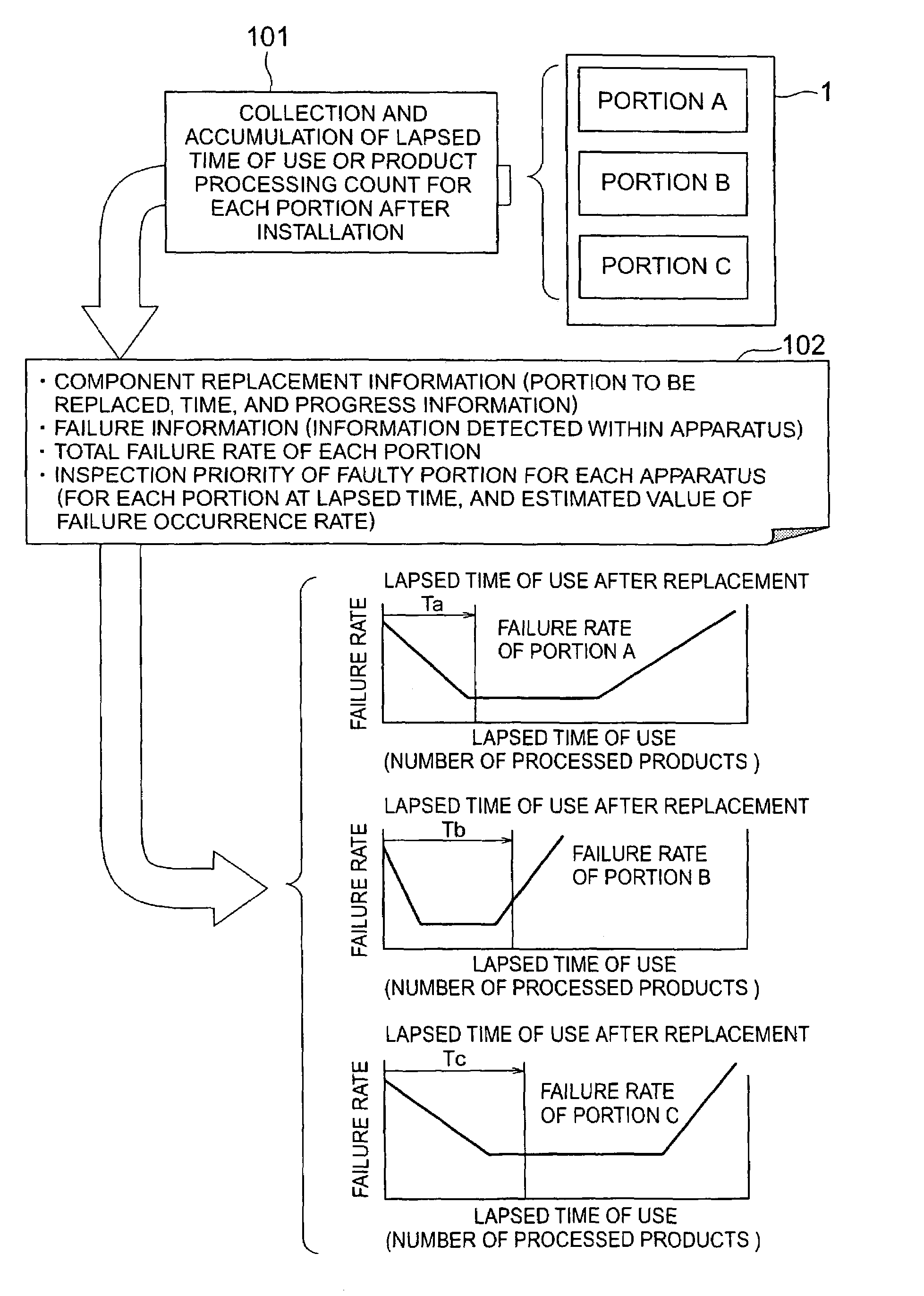
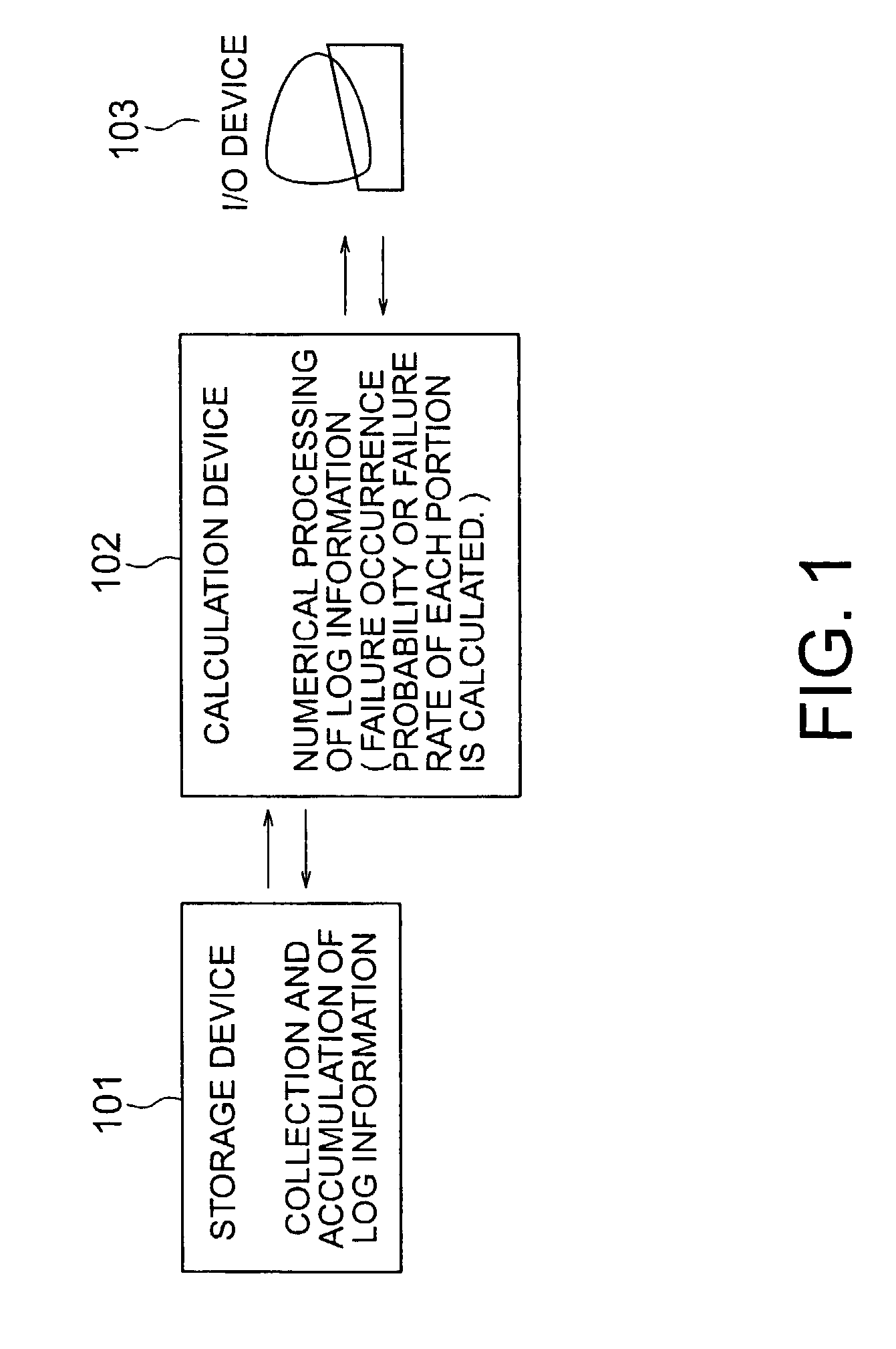
[0089]FIG. 1 shows the arrangement of a management apparatus regarding occurrence of a failure that is incorporated in a semiconductor manufacturing apparatus according to the first embodiment of the present invention, or the arrangement of a management apparatus for managing a failure generated in a semiconductor manufacturing apparatus which does not incorporate any management apparatus. This management apparatus comprises a storage device 101, calculation device 102, and I / O device 103.

[0090]Log information (to be described later) input from the I / O device 103 is supplied to the storage device 101 and accumulated in it.

[0091]The log information is supplied to the calculation device 102 and calculated. The result is stored in the storage device 101 and output from the I / O device 103.

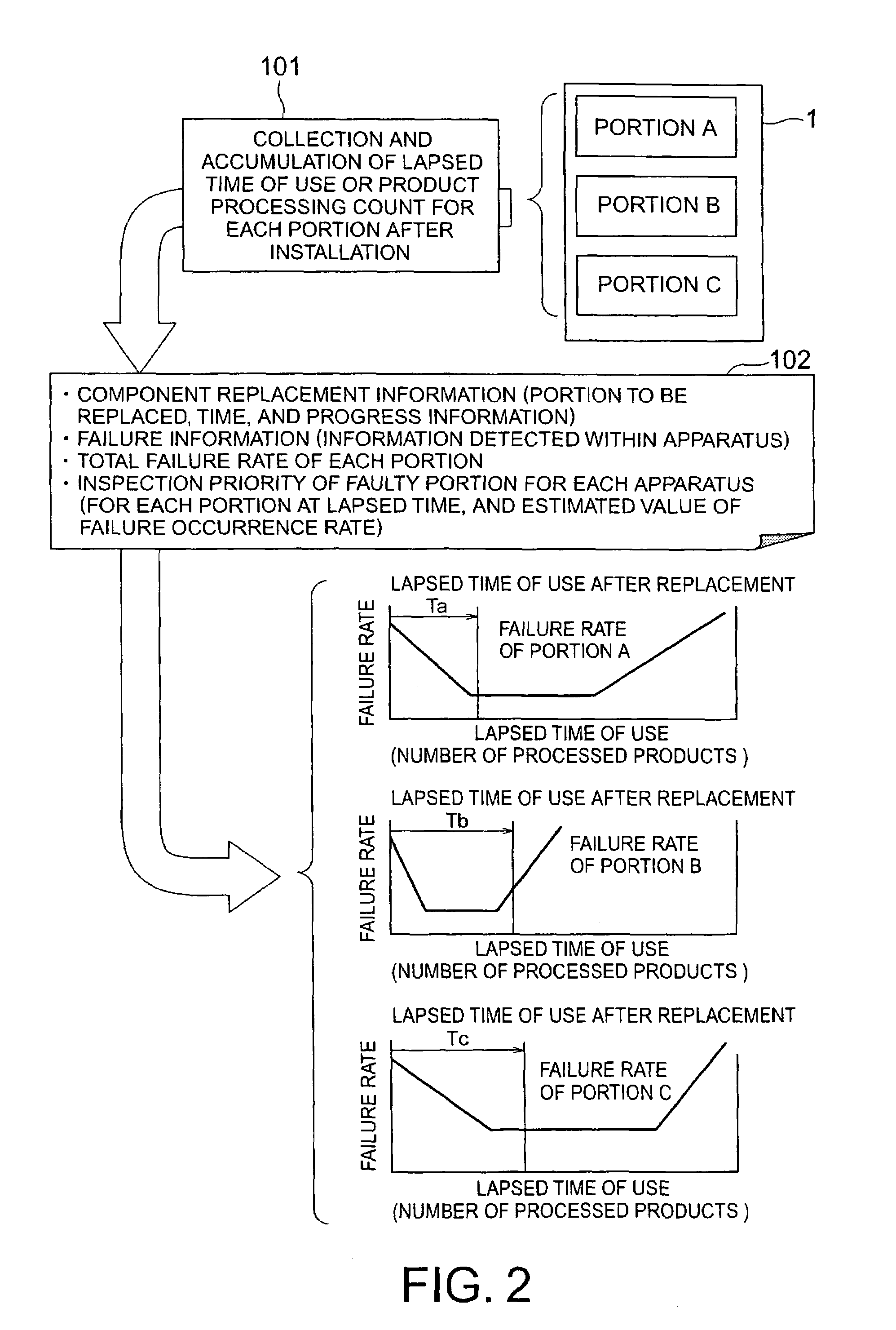
[0092]The processing contents of the management apparatus will be explained with reference to FIGS. 2 and 3.

[0093]As shown in FIG. 2, the lapsed time of use after installation or th...

second embodiment

(2) Second Embodiment

[0111]In the second embodiment of the present invention, the failure probability and / or failure rate is obtained for each portion, similar to the first embodiment. Further, a statistical distribution model is created using histogram information shown in FIG. 4 or information on the number of generated failures as a function of the lapsed time of use, and the estimated value of a failure probability or failure rate as a function of an arbitrary lapsed time of use is calculated.

[0112]FIG. 10 shows an example of applying a Weibull distribution to the histogram in FIG. 4. In FIG. 10, a curve 110 is the line of the Weibull distribution.

[0113]The distribution model applicable to the second embodiment is not limited to the Weibull distribution, and can be a normal distribution, exponential distribution, lognormal distribution, or the like. The applicability of each distribution is desirably taken into consideration.

[0114]FIGS. 11A, 11B, 11C, and 11D show examples of gr...

third embodiment

(3) Third Embodiment

[0121]A semiconductor wafer storage vessel transport apparatus according to the third embodiment of the present invention will be described with reference to FIGS. 13A to 16B.

[0122]An example of the semiconductor wafer storage vessel transport apparatus according to the third embodiment has an outer arrangement shown in FIG. 13A, and a block arrangement shown in FIG. 13B.

[0123]A transport apparatus 407 comprises a transport vehicle 405 having a truck portion 403 including a motor / wheel / battery 408 and a transfer portion 404 including a motor / arm / finger 409, and a controller 406 which controls the operation of the transport vehicle 405.

[0124]FIGS. 14A and 14B show another example of the transport apparatus. Unlike the apparatus shown in FIGS. 13A and 13B, the transport vehicle 405 travels on a track 411.

[0125]FIGS. 15A and 15B show still another example of the transport apparatus. The transport vehicle 405 travels on a track 421, similar to the apparatus shown in ...


PUM


Abstract

A semiconductor manufacturing apparatus having a plurality of portions according to this invention includes a storage device which stores, for each portion, information representing the lapsed time of use or the product processing count till occurrence of a failure after installation of the portion, and a calculation device which receives the information stored in the storage device and outputs function information representing a failure probability and/or failure rate as a function of the lapsed time of use or the product processing count for each portion.

Description

CROSS REFERENCE TO RELATED APPLICATION[0001]This application is based upon and claims benefit of priority under 35 USC 119 from the Japanese Patent Application No. 2002-58489, filed on Mar. 5, 2002, the entire contents of which are incorporated herein by reference.BACKGROUND OF THE INVENTION[0002]The present invention relates to a semiconductor manufacturing apparatus, management apparatus therefor, component management apparatus therefor, and semiconductor wafer storage vessel transport apparatus.[0003]If a failure occurs in a semiconductor manufacturing apparatus and production cannot continue on a semiconductor device manufacturing line, the manufacture of a product during production by the apparatus stops, resulting in a product manufacturing delay or a long product manufacturing term. The generated failure is dealt with by specifying a portion within the apparatus as a failure cause and replacing the faulty portion with a new one.[0004]To specify a faulty portion, a portion whi...

Claims


Application Information

Patent Timeline
Patent Type & Authority Patents(United States)
IPC IPC(8): G06F17/50G06F11/30G06F19/00G05B19/418B65G1/137B65G61/00G05B19/4065H01L21/02H01L21/677
CPCG05B19/4065G05B2219/37253Y02P90/80
Inventor YAJIMA, HIROMISUGANUMA, TATSUMIYOSHIKAWA, NORIAKIYOTSUMOTO, TADASHINAKATA, KENJI
Owner KK TOSHIBA
Why Eureka
Try Eureka