Flexible circuit connector for stacked chip module

a flexible circuit and integrated circuit technology, applied in fixed connections, solid-state devices, basic electric elements, etc., can solve the problems of inflexible sockets, inability to implement complex interconnections, and high cost of rail systems

Inactive Publication Date: 2006-06-27
TAMIRAS PER PTE LTD LLC
View PDF251 Cites 78 Cited by
  • Summary
  • Abstract
  • Description
  • Claims
  • Application Information

AI Technical Summary

Benefits of technology

[0006]The present invention provides a flexible circuit connector for electrically and thermally coupling adjacent IC packages to one another in a stacked configuration. Each IC package includes: (1) a package having top, bottom, and peripheral sides; (2) external leads that extend out from at least one of the peripheral sides of the package; and (3) an IC inside the package connected to the external leads. In one embodiment, the flexible circuit connector comprises a plurality of discrete conductors that are adapted to be mounted between the upper side of a f

Problems solved by technology

The problem then has arisen with regard to how to create electronic pathways, or buses, for stacked packaged integrated circuits that are physically external to-the integrated circuit package and provide an external communication path from the circuit board to each of the individual integrated circuit devices within the stacked module.
Unfortunately, rail system

Method used


Image

  • Flexible circuit connector for stacked chip module
  • Flexible circuit connector for stacked chip module
  • Flexible circuit connector for stacked chip module

Examples


Embodiment Construction

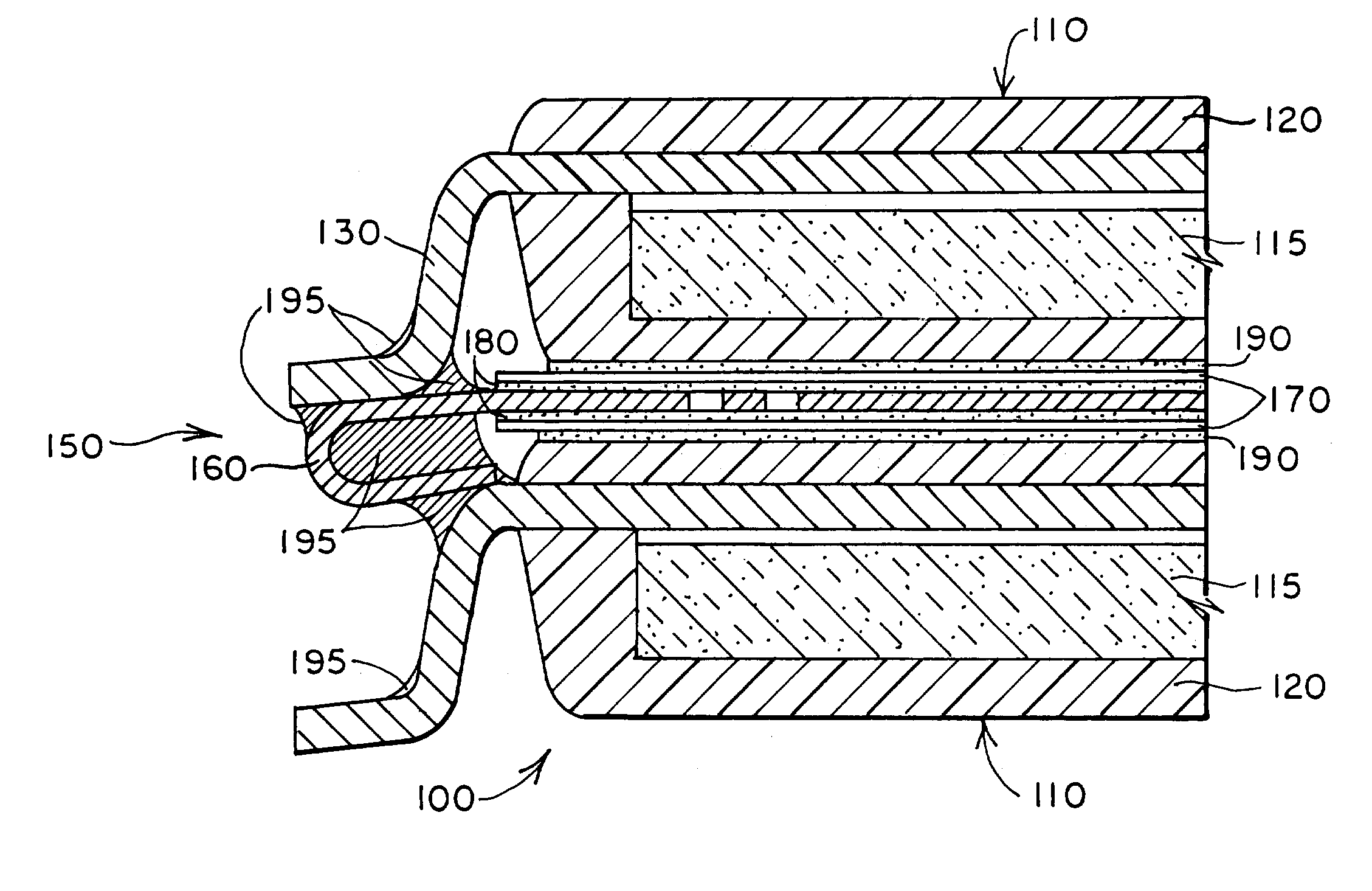
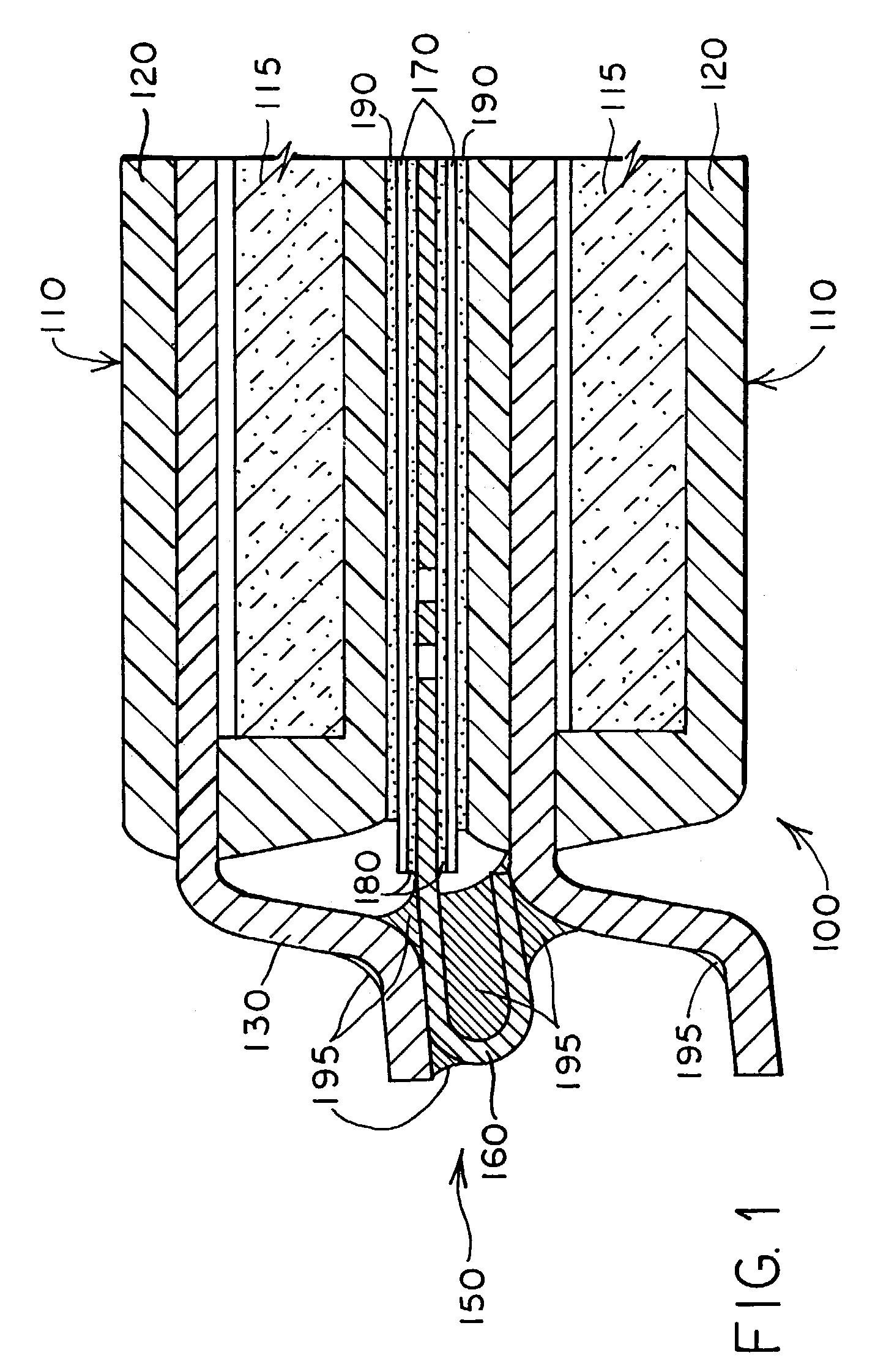
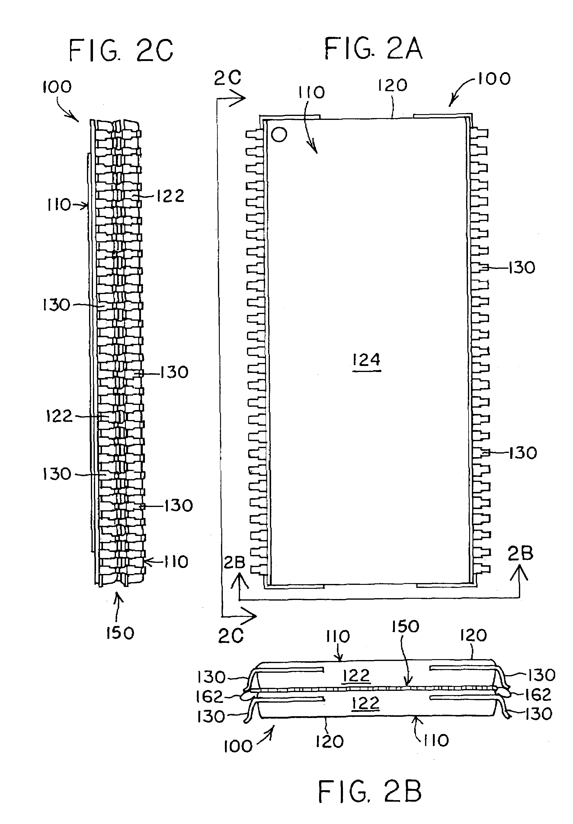
[0016]FIGS. 1 and 2A through 2C show one embodiment of a stacked chip module 100 of the present invention. Module 100 includes first and second IC devices 110 stacked atop and electrically connected to one another through flexible circuit connector 150. Each IC device 110 includes (1) a package 120, (e.g., a plastic package) that protectively encapsulates an internal semiconductor die 115, and (2) external leads 130 extending out from the package 120. Package 120 includes peripheral sides 122 and upper and lower sides 124.

[0017]The depicted flexible circuit connector 150 comprises conductor assembly 160 sandwiched between first and second insulator (electrical) layers 170. In the depicted embodiment, flexible circuit connector 150 also includes adhesive element 180 between insulator layers 170 for adherence to conductor assembly 160. Upper and lower packages 120 are mounted against the first (upper) and second (lower) insulator layers 170 of flexible circuit connector 150 through a ...


PUM


Abstract

The present invention provides a flexible circuit connector for electrically coupling IC devices to one another in a stacked configuration. Each IC device includes: (1) a package having top, bottom, and peripheral sides; and (2) external leads that extend out from at least one of the peripheral sides. In one embodiment, the flexible circuit connector comprises a plurality of discrete conductors that are adapted to be mounted between the upper side of a first package and the lower side of a second package. The flexible circuit connector also includes distal ends that extend from the conductors. The distal ends are adapted to be electrically connected to external leads from the first and second packages to interconnect with one another predetermined, separate groups of the external leads. In this manner, individual devices within a stack module can be individually accessed from traces on a circuit card. This flexible capability is beneficial in modules such as memory modules with multiple, stacked memory devices.

Description

[0001]This application is a continuation of U.S. patent application Ser. No. 10 / 101,039, now U.S. Pat. No. 6,572,387, filed Mar. 19, 2002, which is a continuing prosecution application of U.S. patent application Ser. No. 09 / 406,015, filed Sep. 24, 1999, which is now abandoned. Both U.S. Pat. No. 6,572,387 and U.S. patent application Ser. No. 09 / 406,015 are incorporated herein by reference.TECHNICAL FIELD[0002]This invention relates to integrated to circuit devices. More particulary, this invention relates to a flexible circuit connector for a stacked integrated circuit module.BACKGROUND[0003]Designers of computers and other electronic systems constantly strive to miniaturize integrated circuit (“IC”) devices and modules to place more circuits in smaller spaces while operating at higher speeds. Because of this demand, there is a need to develop smaller, yet denser, memory packages, or modules, and other small, yet dense, modules containing integrated circuit devices, such as micropro...

Claims


Application Information

Patent Timeline
IPC IPC(8): H01R12/00H01L23/495H01L25/10
CPCH01L23/49537H01L25/105H01R12/62H01R4/04H01L2225/1029H01L2924/0002H01L2225/107H01L2924/00
Inventor BURNS, CARMEN D.ROPER, DAVIDCADY, JAMES W.
Owner TAMIRAS PER PTE LTD LLC
Why Eureka
Try Eureka