Layout structure of bit line sense amplifier of semiconductor memory device

a memory device and amplifier technology, applied in semiconductor devices, digital storage, instruments, etc., can solve problems such as the disadvantage of achieve the effect of preventing deteriorating characteristic of memory cores and reducing loading differences

Inactive Publication Date: 2006-06-27
SAMSUNG ELECTRONICS CO LTD
View PDF3 Cites 17 Cited by
  • Summary
  • Abstract
  • Description
  • Claims
  • Application Information

AI Technical Summary

Benefits of technology

[0005]A purpose of the present invention provides a layout structure of a bit line sense amplifier of a semiconductor memory device capable of preventing deteriorating characteristic of a memory core due to a loading mismatch by reducing a loading difference between a bit line and a bit bar line.

Problems solved by technology

If the loading of the bit line is different from that of the bit bar line, there is a disadvantage to deteriorate characteristic of a memory core due to a develop difference between the bit line and the bit bar line when the IO switch is turned on.

Method used


Image

  • Layout structure of bit line sense amplifier of semiconductor memory device
  • Layout structure of bit line sense amplifier of semiconductor memory device
  • Layout structure of bit line sense amplifier of semiconductor memory device

Examples


Embodiment Construction

[0022]The present invention will be described more fully hereinafter with reference to the accompanying drawings, in which exemplary embodiments of the invention are shown.

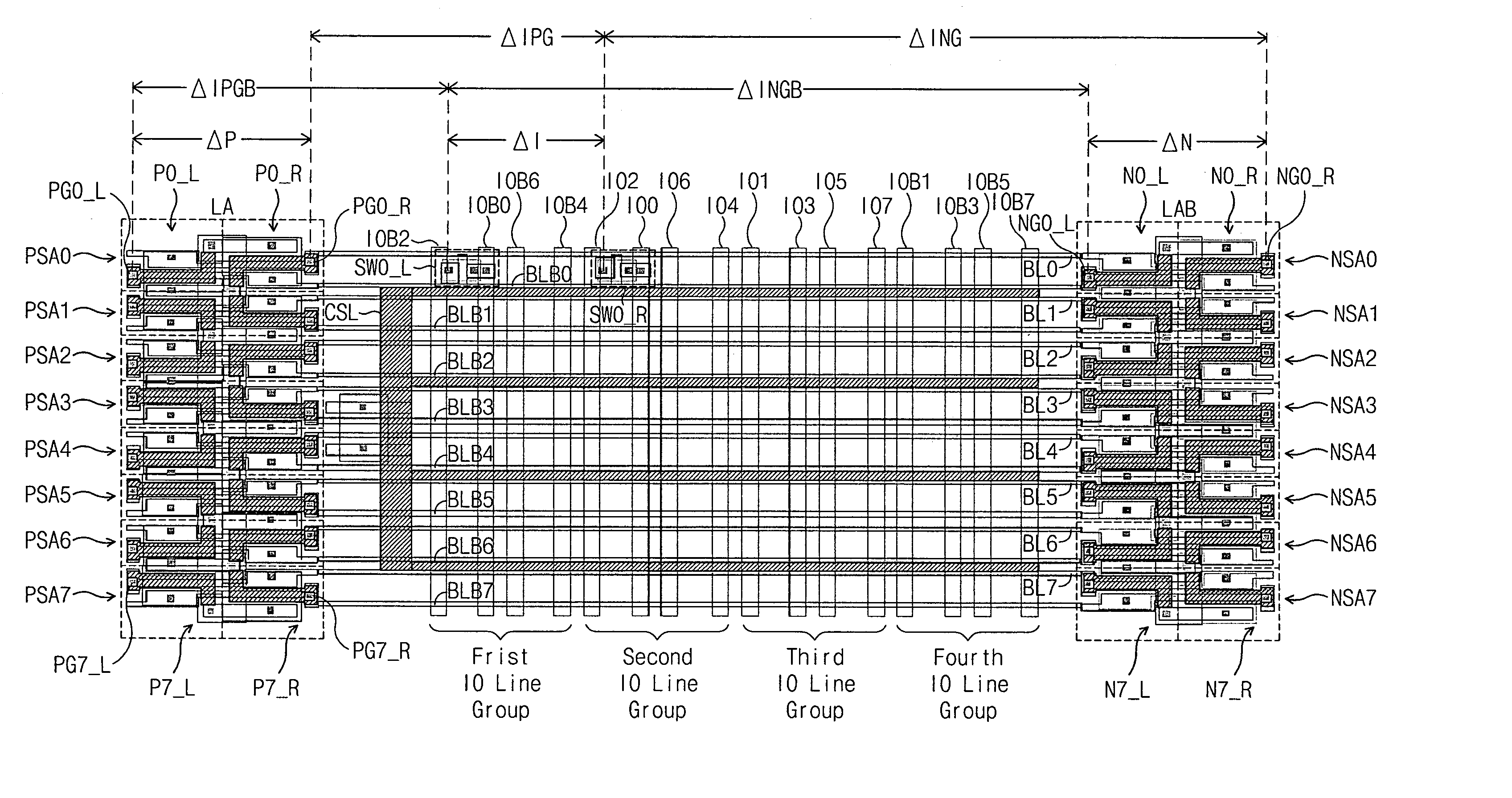
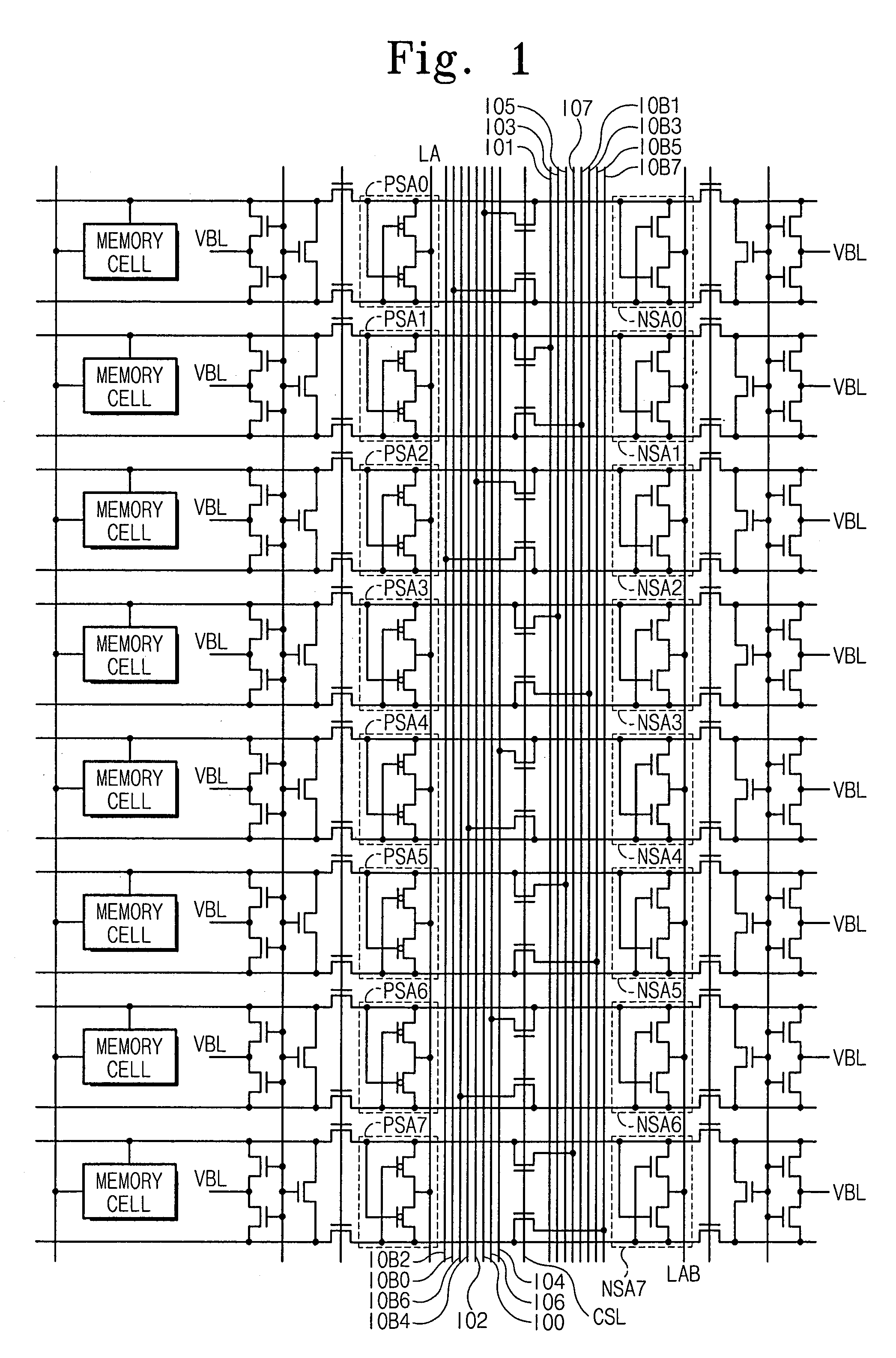
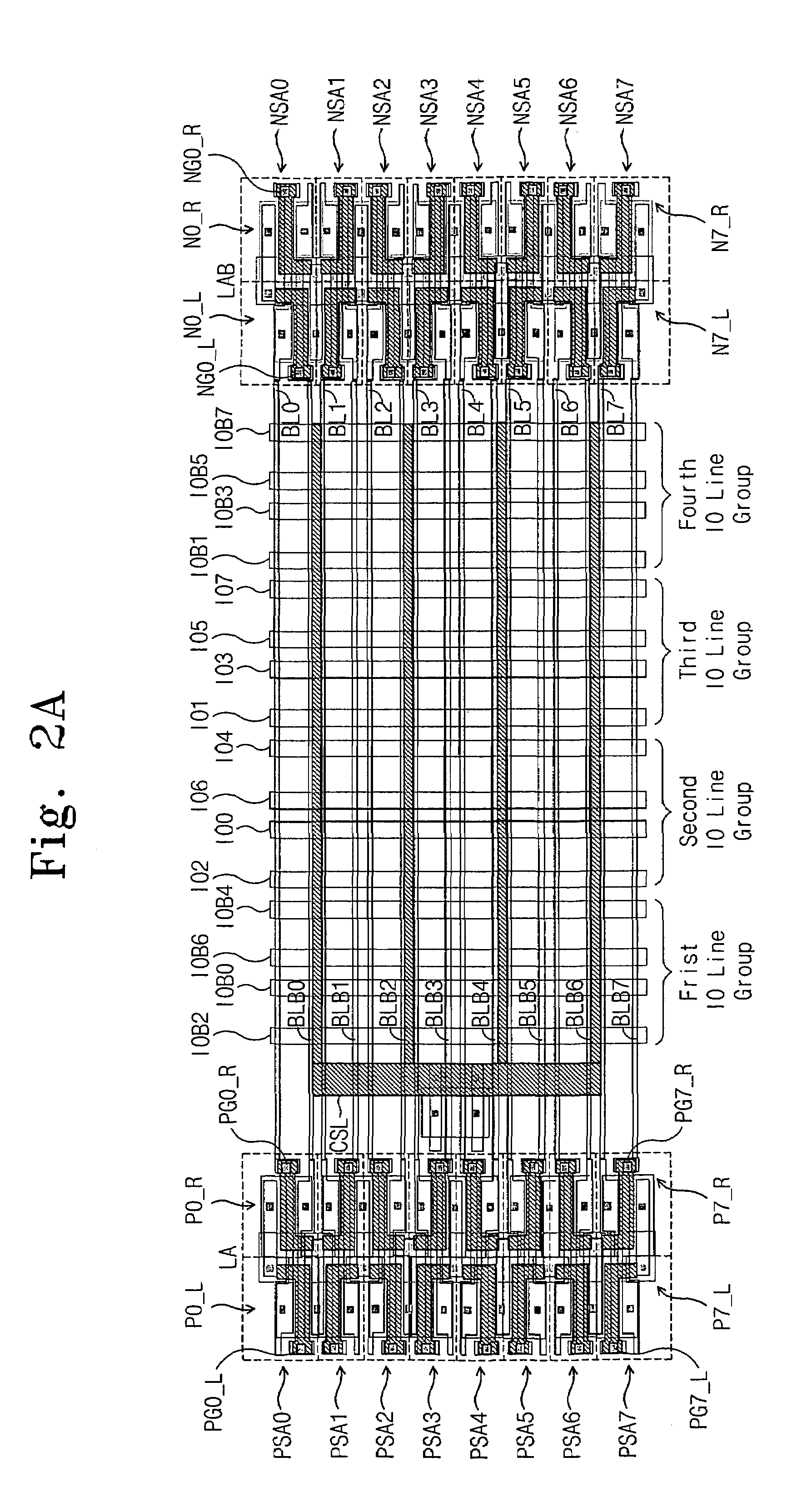
[0023]An embodiment of the present invention is described about a layout structure of a bit line sense amplifier of a semiconductor memory device having eight bit line pairs, eight IO line pairs and sixteenth IO switches with respect to each of sixteenth IO lines.

[0024]FIG. 1 is a view showing construction of the bit line sense amplifier according to an embodiment of the present invention. FIGS. 2A to 2E are views showing the layout structure of the bit line sense amplifier and an arrangement of an IO switch according to an embodiment of the present invention.

[0025]Referring to Figs, the bit line sense amplifier according to an embodiment of the present invention comprises: eight bit line pairs; eight IO line pairs; eight NMOS sense amplifiers; eight PMOS sense amplifiers; and sixteenth IO switches.

[0026]The eight...


PUM


Abstract

A layout structure of a bit line sense amplifier is provided. According to an embodiment of the present invention, the layout structure of the bit line amplifier of a semiconductor memory device includes memory blocks structured by a plurality of cells, bit line pairs connected to the cells and a plurality of bit line sense amplifier blocks for sensing data of the cells, wherein each of the bit line sense amplifier blocks comprises: PMOS sense amplifier structured by first and second PMOS transistors; NMOS sense amplifier structured by first and second NMOS transistors; an IO line pair structured by an IO line and an IO bar line, which are placed between the PMOS sense amplifier and the NMOS sense amplifier; and a first IO switch and a second IO switch, which are connected to one of the bit line pair and the IO line pair, wherein a gate region of the first PMOS transistor, a gate region of the first NMOS transistor and the first IO switch are respectively arranged at a gate region of the second PMOS transistor, a gate region of the second NMOS transistor and the second IO switch in one direction only at predetermined spaces ΔP, ΔN and ΔI.

Description

[0001]This application claims priority from Korean Patent Application No. 2003-85119, filed on Nov. 27, 2003, the contents of which is herein incorporated by reference in its entirety.FIELD OF THE INVENTION[0002]This disclosure generally relates to semiconductor memory devices and, more specifically, to a layout structure of a bit line sense amplifier of a semiconductor memory device.BACKGROUND OF THE INVENTION[0003]A bit line sense amplifier is structured by a PMOS sense amplifier and a NMOS sense amplifier. The bit line sense amplifier amplifies data loaded in a bit line and a bit bar line of a semiconductor memory device, and thereby outputting thereof through an IO line.[0004]In IO lines between the PMOS sense amplifier and the NMOS sense amplifier, and a layout structure of a bit line sense amplifier where an IO switch is arranged to connect the bit line and a bit bar line, a distance difference from a drain of the IO switch to each gate of a NMOS sense amplifier sharing the dr...

Claims


Application Information

Patent Timeline
Patent Type & Authority Patents(United States)
IPC IPC(8): G11C7/00G11C7/18G11C7/06H01L27/02H01L27/105
CPCG11C7/065H01L27/105H01L27/0207G11C7/18
Inventor WON, JONG-HAK
Owner SAMSUNG ELECTRONICS CO LTD
Why Eureka
Try Eureka