Thin-film transistor and process for its fabrication

a thin film transistor and fabrication process technology, applied in the direction of transistors, semiconductor devices, electrical devices, etc., can solve the problems of reducing electron mobility, increasing the effective channel length, increasing the interface trap level, etc., and achieving the effect of preventing deterioration of its characteristics

Active Publication Date: 2010-03-11
CANON KK
View PDF20 Cites 56 Cited by
  • Summary
  • Abstract
  • Description
  • Claims
  • Application Information

AI Technical Summary

Benefits of technology

[0011]In the present invention, at the interface between the gate electrode and the gate insulating layer, the difference between hill tops and dale bottoms of unevenness in the vertical direction of the interface is controlled within a specific numerical range so that the intended effect can be brought out. Stated specifically, the difference between hill tops and dale bottoms of unevenness in the vertical direction of the interface is so controlled as to be 30 nm or less, preferably 3.0 nm or less, and most preferably 1.0 nm or less. Making the interface have such evenness or smoothness that satisfies the above numerical range can provide a thin-film transistor kept from any deterioration of thin-film transistor characteristics which is otherwise caused by the unevenness of the interface between the gate insulating layer and the semiconductor layer. According to the thin-film transistor fabrication process of the present invention, the unevenness of the interface between the gate electrode and the gate insulating layer can be controlled, and hence the thin-film transistor can be kept from deterioration of its characteristics.

Problems solved by technology

H06-045605 discloses a problem that any unevenness of an interface between the gate insulating layer and the semiconductor layer may cause a lowering of electron mobility.
The unevenness of an interface between the gate insulating layer and the semiconductor layer is also considered to cause an increase in interface trap level, an increase in effective channel length, unevenness of layer thickness of the semiconductor layer, stepped-cut of the semiconductor layer, and so forth.
On the other hand, the amorphous ITO thin films have an inferior electric conductivity, and hence the polycrystalline ITO thin films are commonly used for electrodes.
However, if the ITO thin film is formed as a transparent gate electrode under such conditions that it comes to have the polycrystalline form at the time its formation has been completed, a large unevenness reflecting the crystal habit of crystal grains may inevitably come about on the surface of the thin film obtained.
As stated above, if a semiconductor layer is formed on such a gate insulating layer having a large surface unevenness, the interface between the gate insulating layer and the semiconductor layer becomes greatly uneven to inevitably cause deterioration of thin-film transistor characteristics.
Thus, in a bottom gate type thin-film transistor in which the gate insulating layer, the semiconductor layer, the source electrode / drain electrode and the protective layer are formed in this order on the gate electrode, there has been a problem that any sufficient characteristics are not obtainable when the polycrystalline ITO thin film is used as the gate electrode.

Method used


Image

  • Thin-film transistor and process for its fabrication
  • Thin-film transistor and process for its fabrication
  • Thin-film transistor and process for its fabrication

Examples


example 1

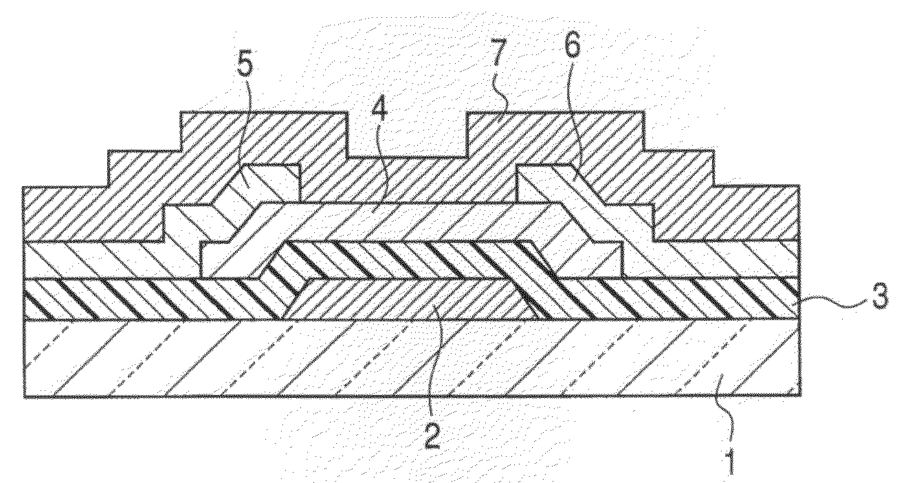
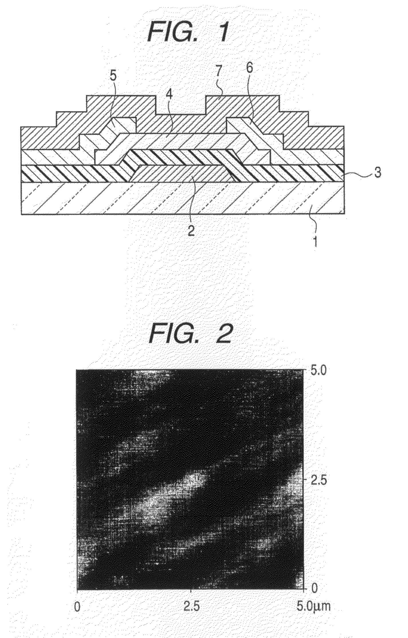
[0049]This Example is an example in which the bottom gate type thin-film transistor shown in FIG. 1 is fabricated. In the thin-film transistor shown in FIG. 1, the layers are formed on the substrate 1 in order. Stated more specifically, the gate electrode 2, the gate insulating layer 3, the semiconductor layer 4, the source electrode 5 / drain electrode 6 and the protective layer 7 are formed on the substrate 1 in this order.

[0050]A glass substrate (1737, available from Corning Glass Works) was used as the substrate 1. The glass substrate was 0.5 mm in thickness.

[0051]First, an amorphous conductive oxide layer was formed on the substrate 1. In this Example, an amorphous ITO thin film was formed by RF magnetron sputtering in an atmosphere of a mixed gas of argon gas and oxygen gas. The ratio of In:Sn was 91:9. In this Example, a polycrystalline sintered body of 3 inches in size was used as a target (material source), and applied RF power was 100 W. The atmosphere at the time of film fo...

example 2

[0070]This Example is an example in which the bottom gate type thin-film transistor shown in FIG. 1 is fabricated. In the thin-film transistor shown in FIG. 1, the layers are formed on the substrate 1 in order. Stated more specifically, the gate electrode 2, the gate insulating layer 3, the semiconductor layer 4, the source electrode 5 / drain electrode 6 and the protective layer 7 are formed on the substrate 1 in this order.

[0071]A glass substrate (1737, available from Corning Glass Works) was used as the substrate 1. The glass substrate is 0.5 mm in thickness.

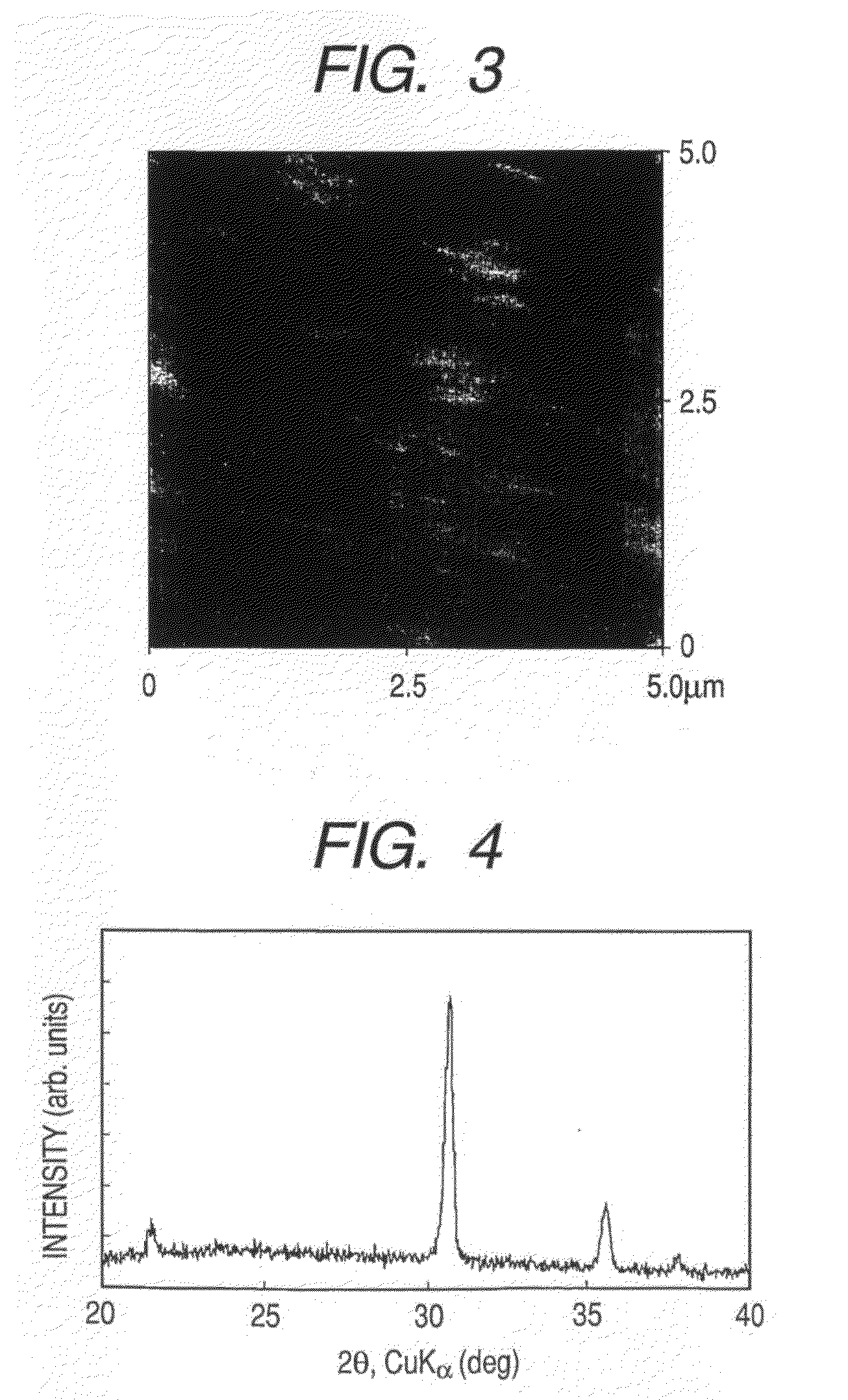
[0072]First, a polycrystalline ITO thin film was formed on the substrate 1. In this Example, the polycrystalline ITO thin film was formed by RF magnetron sputtering in an atmosphere of a mixed gas of argon gas and oxygen gas.

[0073]The ITO thin film thus formed was observed by XRD to obtain the result shown in FIG. 6. Clear diffraction peaks showing a crystalline state were seen, to find that the ITO thin film obtained was in a ...


PUM


Abstract

A bottom gate type thin-film transistor constituted of at least a substrate, a gate electrode, a gate insulating layer, a semiconductor layer, a source electrode and a drain electrode. At an interface between the gate electrode and the gate insulating layer, the interface has a difference between hill tops and dale bottoms of unevenness in the vertical direction, of 30 nm or less.

Description

TECHNICAL FIELD[0001]This invention relates to a thin-film transistor and a process for its fabrication. More particularly, it relates to a bottom gate type thin-film transistor which is transparent to visible light and a process for its fabrication.BACKGROUND ART[0002]In recent years, at an aim for the application of pixel circuits of liquid-crystal displays and organic electroluminescent displays, development is energetically made on semiconductor elements transparent to visible light which have thin-film transistors making use of transparent oxide semiconductors in active layers.[0003]A thin-film transistor element currently in common use is shown in FIG. 1 as a sectional view. First, a gate metal is formed on an insulating substrate 1, and is then patterned in a desired shape to form a gate electrode 2. On this gate electrode, a gate insulating layer 3, a semiconductor film 4, a source electrode 5 and a drain electrode 6 are formed in this order, thus a thin-film transistor elem...

Claims


Application Information

Patent Timeline
Patent Type & Authority Applications(United States)
IPC IPC(8): H01L29/786H01L21/336
CPCH01L29/7869H01L29/4908
Inventor TAKAHASHI, KENJIHAYASHI, RYOSANO, MASAFUMI
Owner CANON KK
Why Eureka
Try Eureka