MMIC package

Inactive Publication Date: 2000-09-26
STMICROELECTRONICS SRL +1
View PDF3 Cites 61 Cited by
  • Summary
  • Abstract
  • Description
  • Claims
  • Application Information

AI Technical Summary

Problems solved by technology

In this case, its characteristics may be deteriorated during the mounting of the MMIC on the package even if the frequency range of the MMIC is designed to be broad because the frequency range capable of conducting the impedance matching is narrowed.
However, several problems arise for putting the above minimum connection length technique employing the bump to the practical use.
A first problem is that a bypass capacitor which depresses the impedance of the source line to a low level cannot be located just beneath the source terminal of the MMIC.
Since the interconnect length between the bare chip electrode and the wiring pad on the substrate is short in the flip chip mo

Method used


Image

  • MMIC package
  • MMIC package
  • MMIC package

Examples


embodiment 1

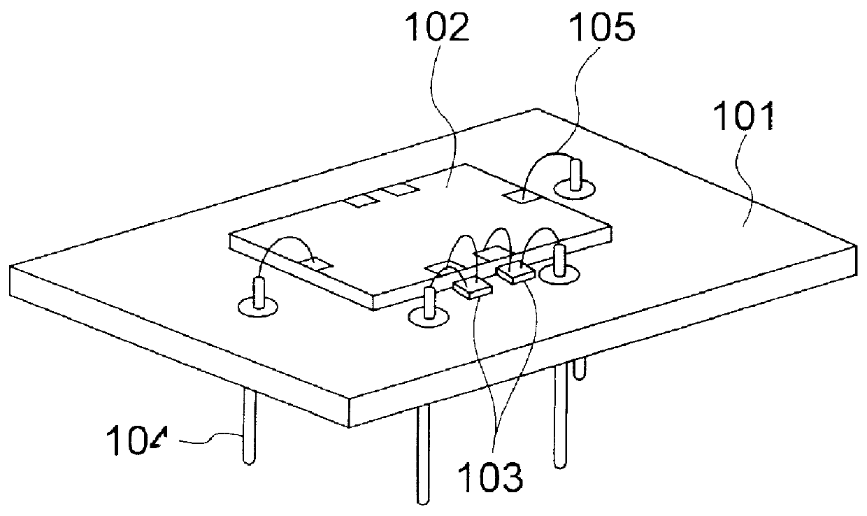
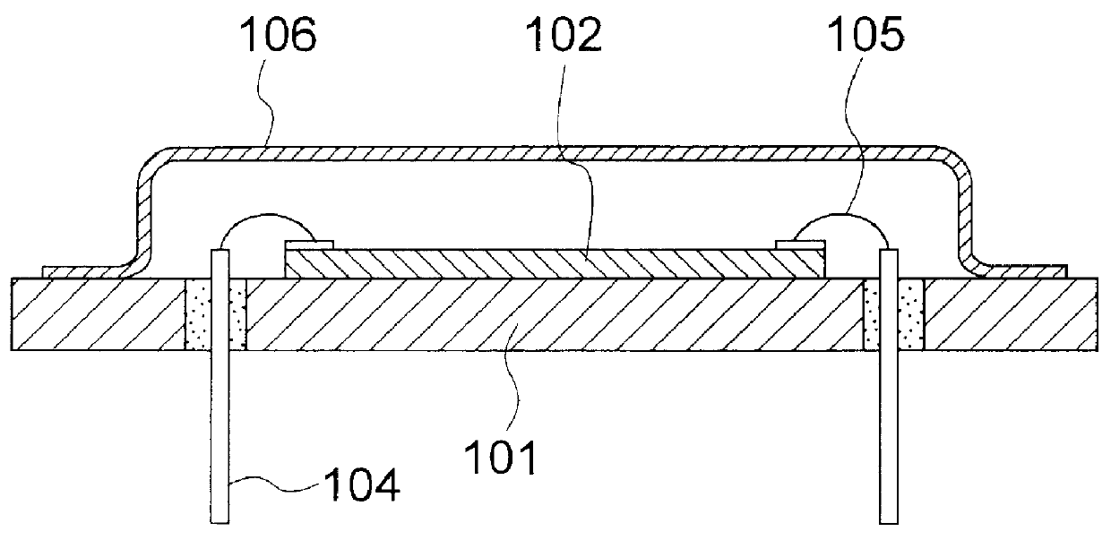
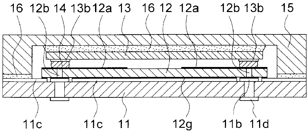
An MMIC package according to the first embodiment shown in FIG. 3 includes base substrate 11 made of ceramics material such as alumina. A signal terminal (not shown) and a source terminal 11b are formed on the top surface of the base substrate 11, and all the surface other than these elements is covered with a planar metal pattern 11c which functions as a GND terminal.

A plurality of pads 11d for connecting with another circuit substrate exist on the bottom surface of the base substrate 11. The respective pads 11d are connected with the above signal terminal (not shown), the source terminal 11b and the planar metal pattern 11c functioning as a GND terminal via through holes. As such, the MMIC package of the present Embodiment takes a so-called LCC (leadless chip carrier) structure.

On the base substrate 11 is mounted a composite capacitor substrate 12 and an MMIC is formed on this composite capacitor substrate 12 by means of the flip chip mounting, that is, by means of face-down bondi...


PUM


Abstract

Disclosed herein is an MMIC package which comprises a base substrate, a composite capacitor substrate made of a ceramics plate mounted on the base substrate, an MMIC bare chip which functions as a high frequency semiconductor element and face-down bonded on the composite capacitor substrate, and an electroconductive covering which covers, together with the base substrate, the MMIC bare chip. In order to suppress the deterioration of the electrical characteristics of the above MMIC, the above components are so arranged that the interconnection length between the components is made to be minimum.

Description

(a) Field of the InventionThe present invention relates to an MMIC (Monolithic Microwave IC) incorporating an MMIC bare chip which is a high frequency semiconductor element.(b) Description of the Related ArtFIG. 1 is a sectional view showing the structure of an example of conventional MMIC packages, and FIG. 2 is a perspective view showing the peripheral structure of MMIC excluding a cap. The conventional MMIC shown in these figures has a metal header 101 made of copper or copper-tungsten, an MMIC 102 die-bonded on the header, and a small plate 103 die-bonded onto the header 101 in the vicinity of a source terminal of the MMIC. The small plate 103 is prepared by plating the both surfaces of a ceramics plate acting as a substrate having a high dielectric constant, and functions as a capacitor formed between the opposing plated surfaces. The power supply from a power source to the MMIC 102, and the input and the output of high frequency signals are performed through external terminals...

Claims


Application Information

Patent Timeline
IPC IPC(8): H01L23/66H01L23/58H01L23/12
CPCH01L23/66H01L2224/16H01L2224/48137H01L2224/4823H01L2224/73253H01L2924/01078H01L2924/01079H01L2924/09701H01L2924/1423H01L2924/16152H01L2924/19041H01L2924/19103H01L2924/30107H01L2924/3011H01L24/48H01L2924/01019H01L2924/01322H01L2224/16225H01L2224/16235H01L2924/00015H01L2224/854H01L2224/45015H01L2224/45144H01L2224/05573H01L2224/05568H01L2224/056H01L2924/00014H01L24/45H01L24/05H01L2224/05599H01L2924/20752
Inventor KUSAMITSU, HIDEKI
Owner STMICROELECTRONICS SRL
Why Eureka
Try Eureka