Eureka AIR delivers breakthrough ideas for toughest innovation challenges, trusted by R&D personnel around the world.

Semiconductor integrated circuit

a technology of integrated circuits and semiconductors, applied in static indicating devices, instruments, optics, etc., can solve the problems of large drain current flows, inability to realize offset states with superior reproducibility, and high cost of substrates, and achieve low cost, high charge holding ability, and sufficient characteristics

Inactive Publication Date: 2007-01-23
SEMICON ENERGY LAB CO LTD
View PDF205 Cites 59 Cited by
  • Summary
  • Abstract
  • Description
  • Claims
  • Application Information

AI Technical Summary

Benefits of technology

[0024]As is understood from the above, it is necessary that all the TFTs be of a P-channel type in a monolithic active matrix circuit that uses offset-gate TFTs in an active matrix circuit (first aspect of the invention). With this configuration, superior circuit characteristics and high reliability have been obtained.
[0025]As described above, in a monolithic active matrix circuit, many electrons are trapped in a TFT using a gate insulating film that was formed at a temperature not higher than 800° C., so that characteristics of an N-channel TFT are greatly deteriorated. Therefore, it is necessary that all the TFTs be of a P-channel type in a monolithic active matrix circuit using TFTs that have a gate insulating film formed at a temperature not higher than 800° C. (second aspect of the invention). With this configuration, superior circuit characteristics and high reliability have been obtained.
[0027]As is understood from the above, it is necessary that all the TFTs be of a P-channel type in a monolithic active matrix circuit that uses offset-gate TFTs in a peripheral drive circuit such as an analog buffer circuit (third aspect of the invention). With this configuration, superior circuit characteristics and high reliability have been obtained.
[0028]As described above, irrespective of an object of forming offset gates, coating gate electrodes with an anodic oxide film is very advantageous. However, the anodic oxide film likely traps charges. In particular, an anodic oxide film left on the side face of a gate electrode, which is close to a gate insulating film, likely traps electrodes and electrons trapped at such locations greatly affect the characteristics when TFTs are of an N-channel type. Therefore, it is necessary that all the TFTs be of a P-channel type in a monolithic active matrix circuit having TFTs in which an anodic oxide film is left on the side face of the gate electrode (fourth aspect of the invention). With this configuration, superior circuit characteristics and high reliability have been obtained.

Problems solved by technology

To obtain such TFTs, the conventional semiconductor manufacturing technologies may be employed as they are, in which case, however, a substrate material should endure a high temperature of more than 900° C. However, such a material is limited to quarts glass, with which the substrate cost is very high when it is of a large area.
On the other hand, because thermal oxidation films as used in ordinary semiconductor processes cannot be used as a gate insulating film, a film of a silicon dioxide, silicon nitride, silicon oxy-nitride, or a like material is used that is formed at a temperature lower than 800° C. by vapor phase deposition such as plasma CVD, atmospheric pressure CVD, or sputtering.
On the other hand, TFTs using non-crystalline silicon such as polycrystalline silicon has a problem that a large drain current (leak current) flows when the gate electrode is reversely biased.
In the past, it was impossible to realize such an offset state with superior reproducibility by a photolithographic process.
However, an insulative film formed by vapor deposition suffers from low film quality.
Further, due to insufficient junction performance of the boundary between the surface of a silicon film and a gate insulating film, there occur many charge trap centers (particularly electron trap centers) at the boundary between the silicon film and the insulating film and in the insulating film.
Therefore, when TFTs using such a material are used for a long time, many electrons are trapped by the trap centers, deteriorating characteristics of the TFTs.
This will deteriorate characteristics of TFTs when they are used for a long time.
However, because a weak-P-type region formed in the offset region is not much influenced by the gate electrode and is far away from the drain region, it is completely uncontrollable.
An anodic oxide film formed around the gate electrode has similar problems.
That is, the above-described N-channel TFT cannot be used for applications that require the threshold voltage to be stable, for instance, switching elements in an active matrix circuit or analog switch elements in peripheral drive circuits for the active matrix circuit.
Due to the above problems, a complementary (CMOS) circuit composed of N-channel TFTs and P-channel TFTs has a problem that it does not work properly after long-term usage because of deterioration of the N-channel TFTs.

Method used


Image

  • Semiconductor integrated circuit
  • Semiconductor integrated circuit
  • Semiconductor integrated circuit

Examples


embodiment 1

[0040]A description will be made of an embodiment in which a monolithic liquid crystal display is produced according to the present invention. FIG. 8 is a block diagram showing a monolithic liquid crystal display according to this embodiment. All of TFTs used in component circuits of a liquid crystal display, i.e., a shift register X (for a source driver), a shift register Y (for a gate driver), analog switches of the source driver, and other peripheral circuits and an active matrix circuit are of a P-channel type. FIG. 5 is a circuit diagram showing the shift register (one stage) of this embodiment.

[0041]This circuit requires three power lines VDD, VSS and VGG, where VDD>VSS. An optimum value of VGG is determined considering characteristics of the TFTs and, preferably, is approximately equal to or smaller than VSS.

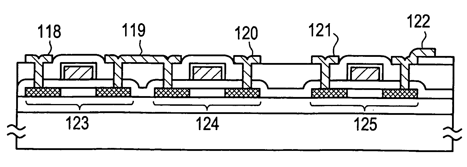
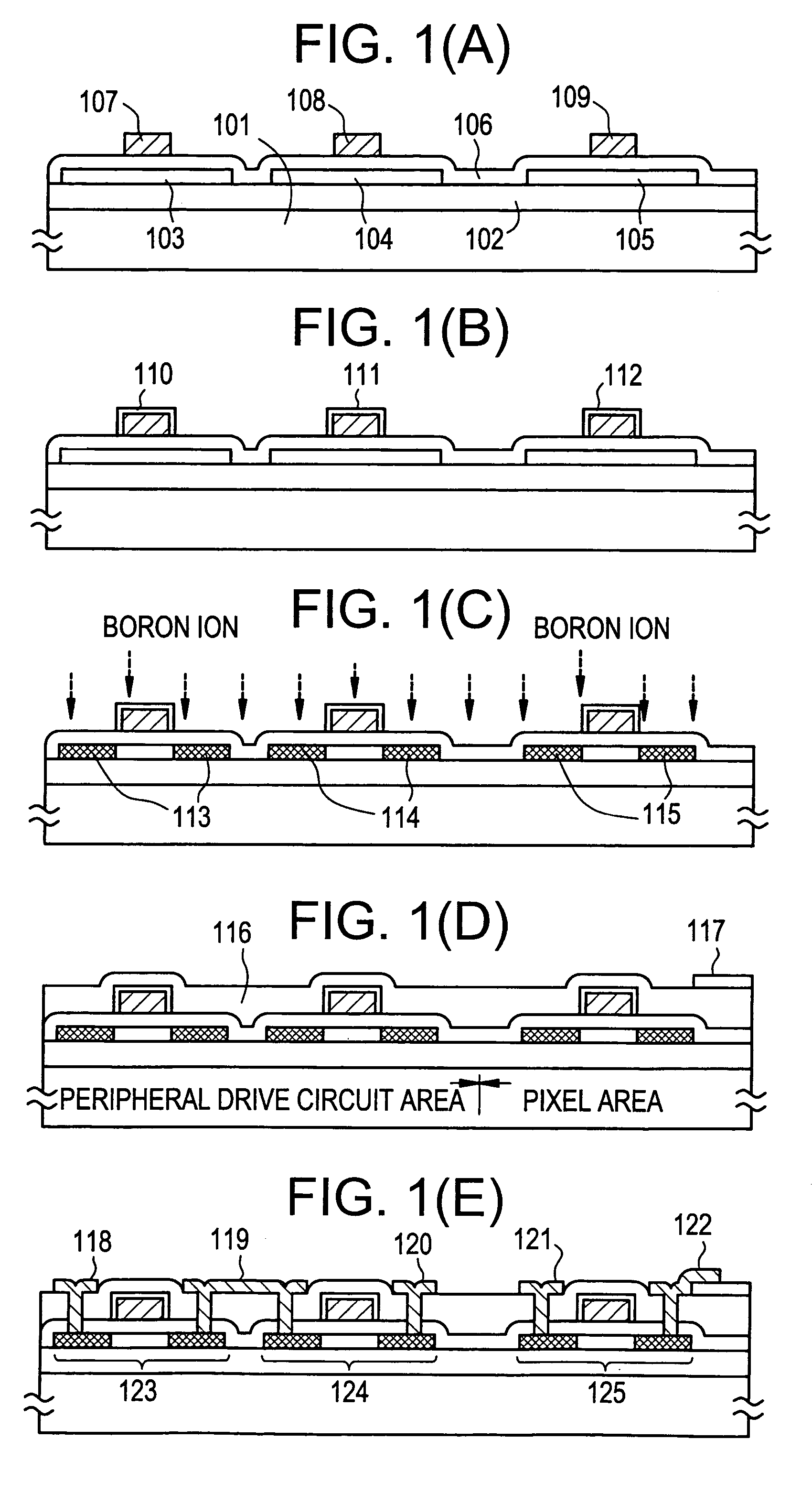
[0042]Referring to FIGS. 1(A)–1(E), a description will be made of a circuit manufacturing process of the above monolithic liquid crystal display. It is desirable that a s...

embodiment 2

[0052]A description will be made of an embodiment in which another monolithic liquid crystal display is produced according to the invention. A block diagram of a monolithic liquid crystal display of this embodiment is the same as that of FIG. 8. FIG. 6 is a circuit diagram showing a shift register (one stage) of this embodiment. While all the TFTs are of a P-channel type, this embodiment has a feature that depletion type TFTs are used as loads in addition to enhancement type TFTs. In this circuit, only two power lines VDD and VSS are used; that is, the power line VGG of the first embodiment is not necessary. Therefore, this embodiment is preferable in terms of the circuit integration. The operation speed of this embodiment is generally faster than the first embodiment. The condition VDD>VSS should also be satisfied in this embodiment.

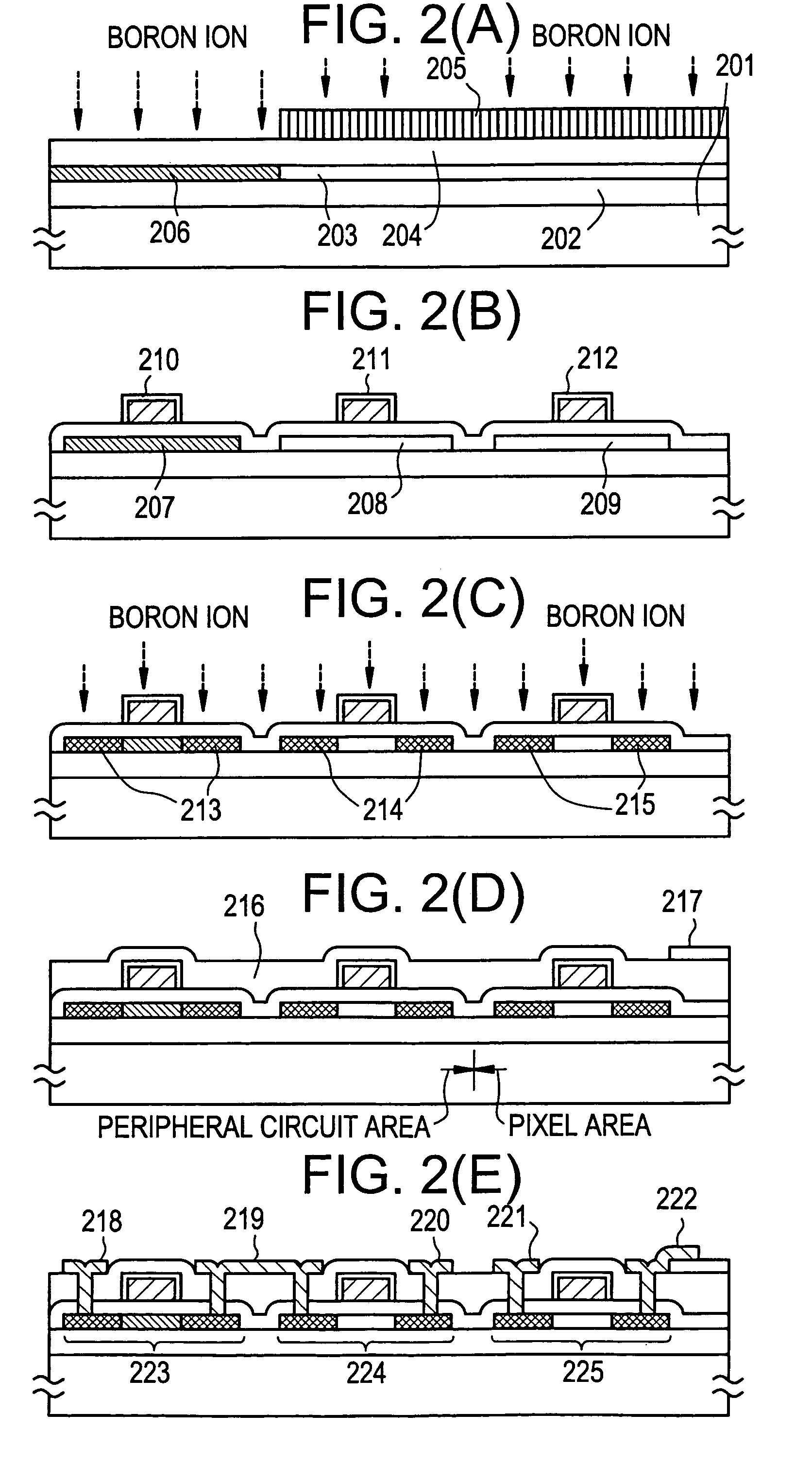
[0053]Referring to FIGS. 2(A)–2(E), a circuit manufacturing process of the above monolithic liquid crystal display will be described. A substrate 201 m...

embodiment 3

[0062]A description will be made of an embodiment in which another monolithic liquid crystal display is produced according to the invention. A block diagram of a monolithic liquid crystal display of this embodiment is the same as that of FIG. 8. FIG. 4 is a circuit diagram showing a shift register (one stage) of this embodiment. While all the TFTs are of a P-channel type, this embodiment has a feature that resistors are used as loads. In this circuit, only two power lines VDD and VSS are used as in the case of the second embodiment. The operation speed of this embodiment is generally faster than the first embodiment. The condition VDD>VSS should also be satisfied in this embodiment.

[0063]FIGS. 3(A)–3(C) are sectional views of the above-type of circuits, which are manufactured by using the integrated circuit manufacturing technologies as described in the first and second embodiments. Details of a manufacturing process are omitted here.

[0064]Referring to FIG. 3(A), a region 301 is a r...


PUM

PropertyMeasurementUnit
temperatureaaaaaaaaaa
acceleration voltageaaaaaaaaaa

Abstract

In a monolithic active matrix circuit that uses offset-gate TFTs in which the gate electrode is offset from the source and drain regions or TFTs whose gate insulating film is formed by vapor deposition, not only an active matrix circuit but also a drive circuit therefor is formed by using P-channel TFTs.

Description

BACKGROUND OF THE INVENTION[0001]The present invention relates to a semiconductor integrated circuit that is composed of thin-film semiconductor elements. The invention particularly relates to a monolithic active matrix devices, such as a liquid crystal display device and a dynamic RAM (DRAM), which have a matrix structure and in which an active matrix circuit including MOS or MIS (metal-insulator-semiconductor) field-effect elements (generally called MOS elements) that serve as switching elements for the matrix structure and a drive circuit for driving the active matrix circuit are formed on a single substrate. Further, the invention particularly relates to a device which uses thin-film transistors that are formed as MOS elements on an insulative surface at a relatively low temperature.[0002]In recent years, in display devices having a matrix structure such as a liquid crystal display, studies have been made intensively of a matrix circuit (active matrix circuit) that uses thin-fil...

Claims


Application Information

Patent Timeline
Patent Type & Authority Patents(United States)
IPC IPC(8): H01L29/04H01L29/10H01L29/15H01L31/036H01L31/0376H01L31/20G02F1/133G02F1/1345G02F1/136G02F1/1368H01L21/336H01L21/77H01L21/84H01L27/12H01L29/49H01L29/78H01L29/786
CPCH01L27/1214H01L29/78621H01L29/4908G02F1/136
Inventor KOYAMA, JUNKAWASAKI, YUJI
Owner SEMICON ENERGY LAB CO LTD
Why Eureka
Eureka Blog
Learn More