On-chip compensation control for voltage regulation

a compensation control and voltage regulation technology, applied in the field of electric circuits for voltage regulation, can solve the problems of sub-threshold conduction, significant leakage current of transistors of such small dimensions,

Inactive Publication Date: 2006-07-11
INNOTECH SYST
View PDF3 Cites 54 Cited by
  • Summary
  • Abstract
  • Description
  • Claims
  • Application Information

AI Technical Summary

Problems solved by technology

Additionally, transistors of such small dimensions tend to have significant leakage current, or sub-threshold conduction.

Method used


Image

  • On-chip compensation control for voltage regulation
  • On-chip compensation control for voltage regulation
  • On-chip compensation control for voltage regulation

Examples


Embodiment Construction

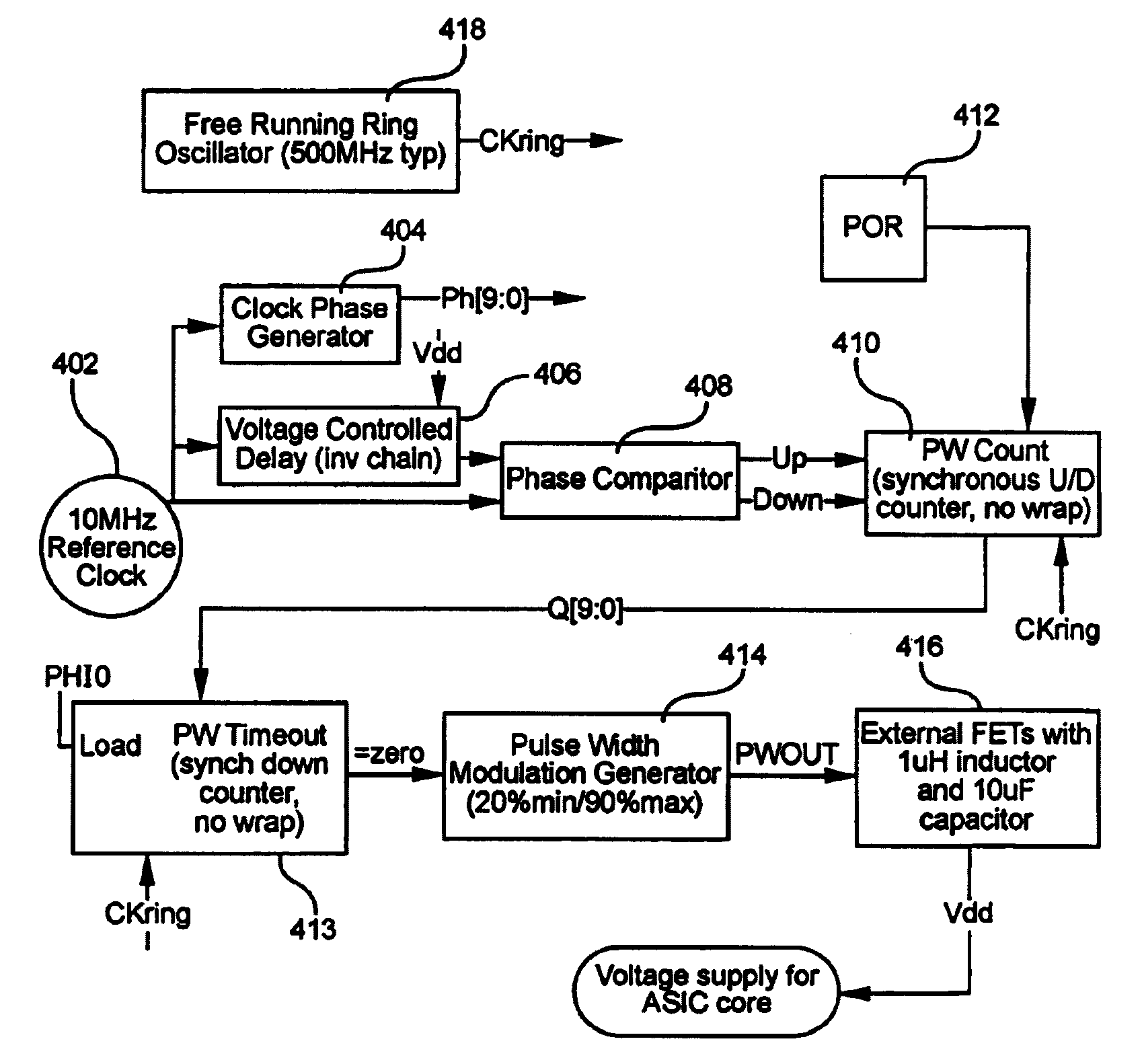
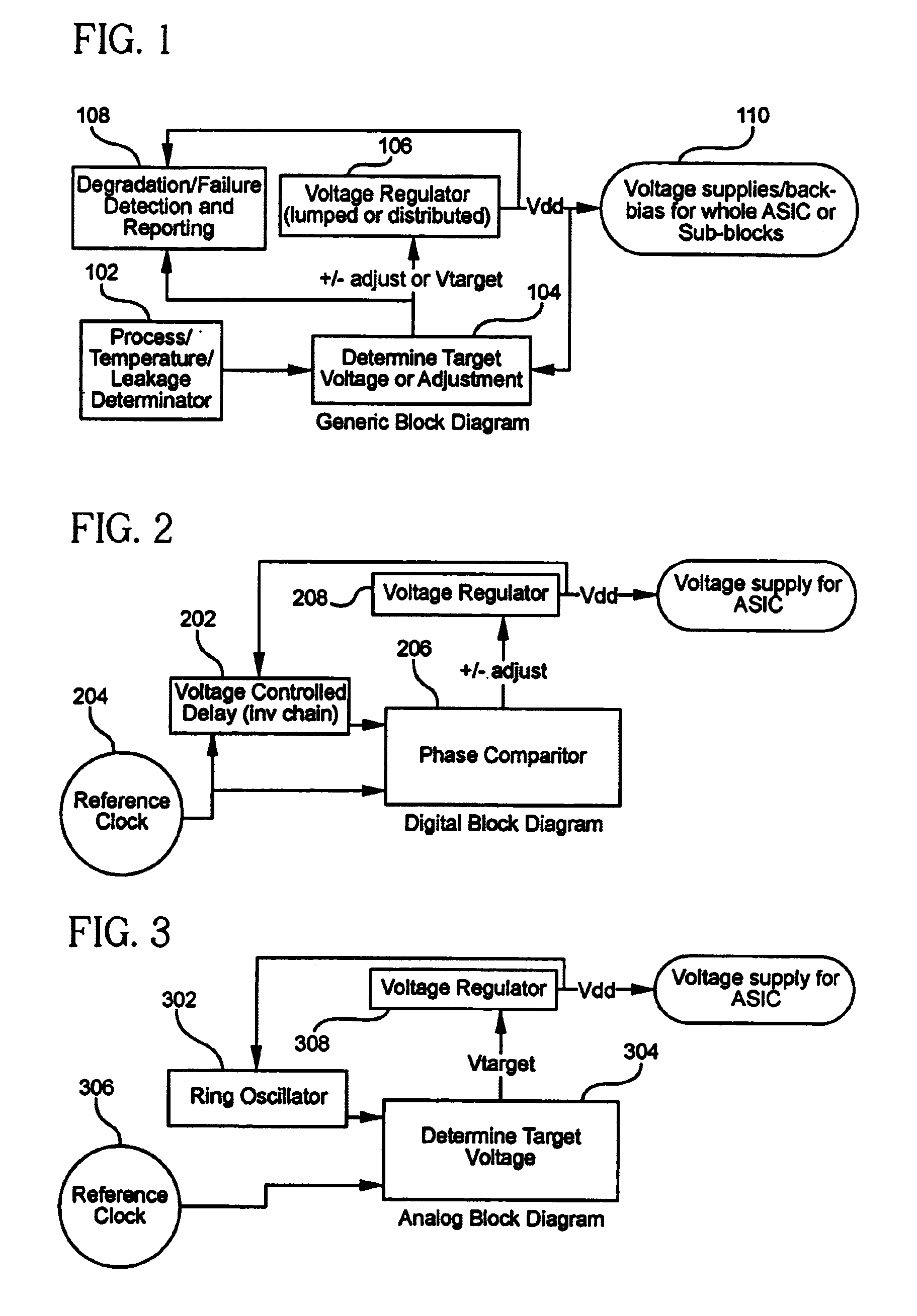
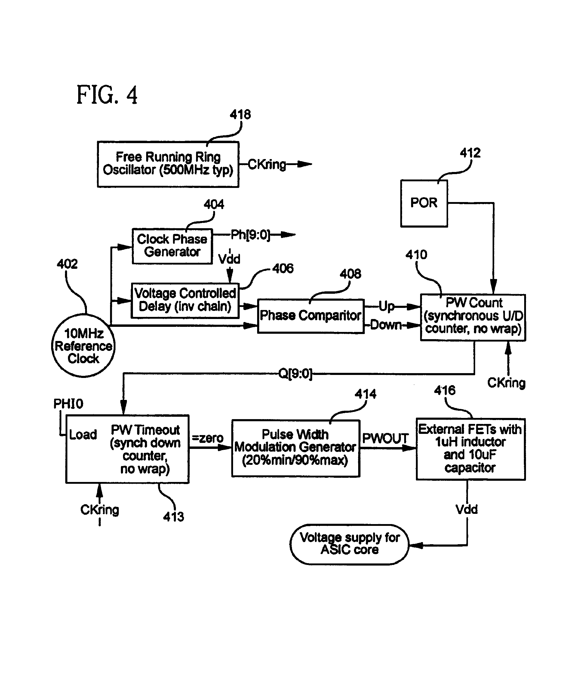
[0019]Various embodiments of the present invention provide control information to a voltage regulator in order to modify, or adjust, the nominal output voltage of such a regulator. These modifications to the nominal output voltage are generally made so as to compensate for manufacturing and / or operational characteristics. In typical embodiments of the present invention, an integrated circuit, which is coupled to receive the regulated output voltage, is “instrumented” so as to provide feedback to the voltage regulator. By way of example, and not limitation, an integrated circuit having transistor performance at the low end of the current-drive range for a particular semiconductor manufacturing process may command the voltage regulator to increase the power supply voltage so as to increase the desired speed of operation. Similarly, if the operational characteristics of the integrated circuit are adversely impacted by ambient temperature, then the control information may command the vo...


PUM


Abstract

Manufacturing and / or operational variations that affect performance of an integrated circuit (IC) are at least partially compensated for, by determining the magnitude of these variations and providing one or more corresponding control signals to a voltage regulator, which, responsive thereto, increases or decreases the magnitude of the output voltage. The output voltage of the voltage regulator is typically provided to a power supply node of the IC. Similarly, the output of the voltage regulator may be provided to a substrate portion of the IC, so as to provide a substrate bias that is variable in response to changes in the performance of the IC. In various embodiments, a determination of the magnitude of the variations is made by comparing the performance of a digital delay circuit or a ring oscillator to a reference clock; speed characterization of the IC may be obtained from the voltage regulator control signals; and information regarding reliability degradation of the IC may be obtained from the control signals that are generated for control of the voltage regulation circuitry.

Description

FIELD OF THE INVENTION[0001]The present invention relates generally to electronic circuits for voltage regulation, and more particularly relates to providing control information to a voltage regulator based upon manufacturing or operational characteristics of an integrated circuit that receives the regulated voltage output of a voltage regulator.BACKGROUND[0002]Advances in semiconductor manufacturing technology have resulted in ever decreasing physical dimensions for the various circuit elements, such as, for example, field effect transistors, which are used in forming integrated circuits. In turn, the smaller dimensions of such circuit elements have allowed the integration onto a single chip of many more transistors than was possible in the past.[0003]As is well-known in the field of integrated circuits, reducing the dimensions of circuit elements generally, and of the field effect transistor (FET) in particular, requires a corresponding reduction in the power supply voltage in ord...

Claims


Application Information

Patent Timeline
Patent Type & Authority Patents(United States)
IPC IPC(8): G05F1/40H02M3/158
CPCH02M3/1588Y02B70/1466H02M2001/0025H02M2001/0022H02M1/0022H02M1/0025Y02B70/10
Inventor MORALES, LOUIS J.
Owner INNOTECH SYST
Why Eureka
Try Eureka