LCD manufacturing method involving forming a main seal pattern by screen printing and a dummy seal pattern by selective dispensing

Active Publication Date: 2006-07-11
LG DISPLAY CO LTD
View PDF178 Cites 5 Cited by
  • Summary
  • Abstract
  • Description
  • Claims
  • Application Information

AI Technical Summary

Benefits of technology

[0032]An advantage of the present invention provides a method for manufacturing a liquid crystal display device having an improved device reliability and decreased tact time.
[0033]Another advantage of the present invention provides a method for manufacturing a liquid crystal display device capable of being applied to Multi-Model-on-a-Glass (MMG) models of liquid crystal display panels having various sizes.

Problems solved by technology

Despite various technical developments in LCD technology, however, research in enhancing picture quality of LCD devices has been lacking compared to research in other features and advantages of LCD devices.
However, use of the aforementioned related art screen printing method is problematic because the amount of sealant material used can be excessive.
Accordingly, a picture quality of the related art LCD device becomes deteriorated.
Use of the aforementioned related art dispensing method of forming the seal pattern is problematic, however, because the main and dummy seal patterns are formed of highly viscous sealant material.
Subsequently, the excessive amount of sealant material accumulated on the nozzle becomes excessively dispensed onto the first substrate.
During bonding of the first and second substrates, the excessively dispensed sealant material spreads toward an active region (center portion of the first substrate) and a dummy region (periphery of the first substrate) and the liquid crystal material becomes contaminated by the sealant material, thereby decreasing device reliability.
Further, use of the related art seal pattern formation methods may become difficult when the size of the first substrate increases, or when a size of the picture display area of the substrate changes (e.g., upon a model change of the liquid crystal display panel).

Method used


Image

  • LCD manufacturing method involving forming a main seal pattern by screen printing and a dummy seal pattern by selective dispensing
  • LCD manufacturing method involving forming a main seal pattern by screen printing and a dummy seal pattern by selective dispensing
  • LCD manufacturing method involving forming a main seal pattern by screen printing and a dummy seal pattern by selective dispensing

Examples


Embodiment Construction

[0049]Reference will now be made in detail to the exemplary embodiments of the present invention, examples of which are illustrated in the accompanying drawings. Wherever possible, the same reference numbers will be used throughout the drawings to refer to the same or like parts.

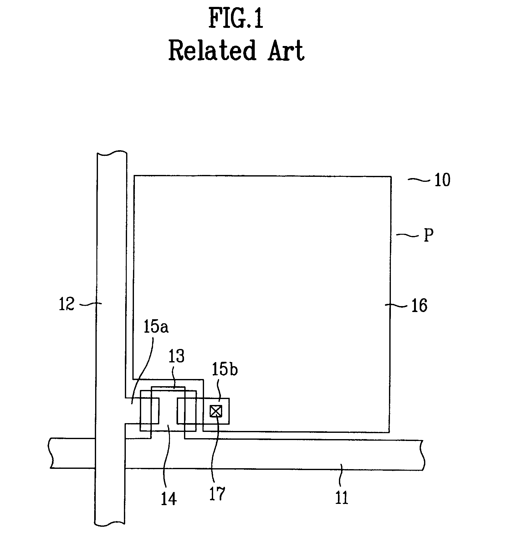
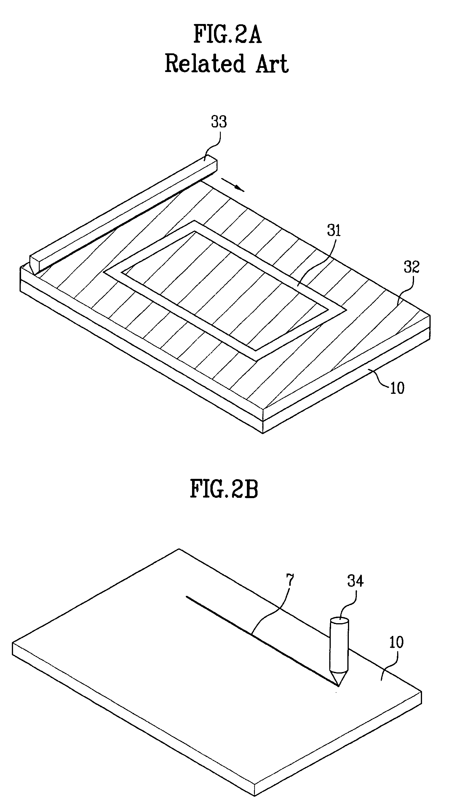
[0050]As sizes of liquid crystal display panels increase, the related art method of manufacturing LCD devices incorporating the liquid crystal injection method has become problematic. More specifically, the amount of time required to completely inject liquid crystal material between two substrates increases as the size of the LCD panel increases. Accordingly, the yield with which LCD devices are manufactured decrease. In order to solve the aforementioned problem, a liquid crystal dispensing method has been proposed in accordance with the principles of the present invention.

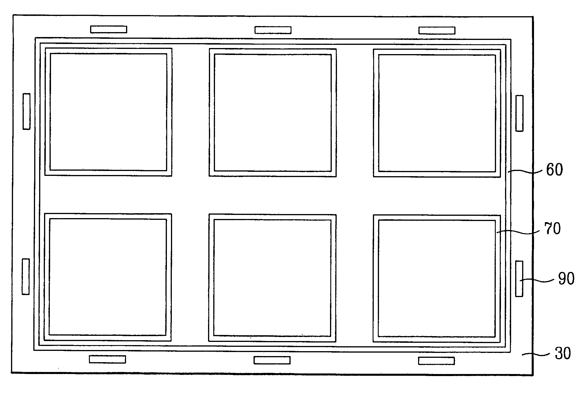
[0051]A method for manufacturing LCD devices using the aforementioned liquid crystal dispensing method will now be described in greater d...


PUM


Abstract

A method for manufacturing a liquid crystal display device includes providing first and second substrates; forming a main seal pattern on one of the first and second substrates by a printing method; forming a dummy sealant on the substrate having the main seal pattern by a selective dispensing method; dispensing liquid crystal material directly onto one of the first and second substrates; attaching the first and second substrates; and irradiating UV light to the attached first and second substrates.

Description

[0001]This application claims the benefit of the Korean Application No. P2002-74819 filed on Nov. 28, 2002, which is hereby incorporated by reference for all purposes as if fully set forth herein. This application incorporates by reference two co-pending application Ser. No. 10 / 184,096, filed on Jun. 28, 2002, entitled “SYSTEM AND METHOD FOR MANUFACTURING LIQUID CRYSTAL DISPLAY DEVICES” and Ser. No. 10 / 184,088, filed on Jun. 28, 2002, entitled “SYSTEM FOR FABRICATING LIQUID CRYSTAL DISPLAY AND METHOD OF FABRICATING LIQUID CRYSTAL DISPLAY USING THE SAME” as if fully set forth herein.BACKGROUND OF THE INVENTION[0002]1. Field of the Invention[0003]The present invention relates to a liquid crystal display (LCD) device, and more particularly, to a method for manufacturing an LCD device while decreasing a tact time.[0004]2. Discussion of the Related Art[0005]With the expansion of the information society, a need has arisen for displays capable of producing high quality images in thin, ligh...

Claims


Application Information

Patent Timeline
IPC IPC(8): G02F1/1339G02F1/13G02F1/1341
CPCG02F1/1341G02F1/1339G02F2001/13415G02F1/13415G02F1/13
Inventor JUNG, SUNG SUKWAK, SO MIN
Owner LG DISPLAY CO LTD
Why Eureka
Try Eureka