Interconnects for semiconductor light emitting devices

Active Publication Date: 2007-03-15
LUMILEDS
View PDF7 Cites 43 Cited by
  • Summary
  • Abstract
  • Description
  • Claims
  • Application Information

AI Technical Summary

Benefits of technology

[0012] Interconnects according to embodiments of the invention may withstand high operating temperatures with reduced degradation or failure, may advantageously lower the thermal and electrical resistance of the connection between the device and the mount by covering

Problems solved by technology

In addition, epoxy has very high thermal resistance, thus the design of FIG. 1 provides only high resistance pathways for heat to escape LED chip 12, limiting device 10 to low power applications.
This is not possible as electrical isolation is required between the p and n el

Method used


Image

  • Interconnects for semiconductor light emitting devices
  • Interconnects for semiconductor light emitting devices
  • Interconnects for semiconductor light emitting devices

Examples


Embodiment Construction

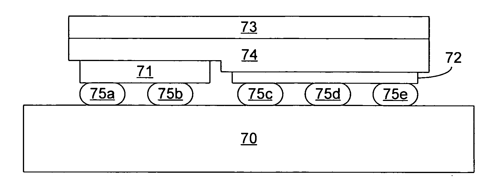
[0021]FIG. 4 illustrates a flip chip light emitting device attached to a mount The flip chip device includes a substrate 73 attached to semiconductor device layers 74, which include at least one light emitting or active layer disposed between an n-type region and a p-type region. N-type contact 71 and p-type contact 72 are electrically connected to the n- and p-type regions of semiconductor structure 74. Semiconductor structure 74 is connected to mount 70 via contacts 71 and 72 by several metal-to-metal interconnects 75a-75e. Mount 70 may be any suitable material including, for example, metals such as copper, semiconductors such as Si, ceramics such as alumina or AIN, or composite mounts such as printed circuit boards and metal core printed circuit boards.

[0022] Metal interconnects 75a-75e are often Al, Au, Cu, or Ni. The interconnects are formed in a stud bumping process where thin metal layers (not shown) are formed on both mount 70 and contacts 71 and 72 at the site of each inte...


PUM


Abstract

A semiconductor light emitting device including a light emitting layer disposed between an n-type region and a p-type region and contacts electrically connected to the n-type region and the p-type region is connected to a mount. A metal layer arbitrarily patterned to cover at least 20% of the area of the semiconductor light emitting device is plated on either a metal layer formed on the mount or a metal layer formed on one of the contacts. The plated metal layer may replace other known interconnecting techniques such as stud bumps. The semiconductor light emitting device is physically connected to the mount by causing interdiffusion between the contact surfaces of the metal layers. In some embodiments, a layer of solder is formed over the plated metal layer, and then the semiconductor light emitting device is physically connected to the mount by heating the solder.

Description

BACKGROUND [0001] 1. Field of Invention [0002] This invention relates to methods of attaching semiconductor light emitting devices to other structures. [0003] 2. Description of Related Art [0004] Semiconductor light-emitting devices including light emitting diodes (LEDs), resonant cavity light emitting diodes (RCLEDs), vertical cavity laser diodes (VCSELs), and edge emitting lasers are among the most efficient light sources currently available. Materials systems currently of interest in the manufacture of high-brightness light emitting devices capable of operation across the visible spectrum include Group III-V semiconductors; for example, binary, ternary, and quaternary alloys of gallium, aluminum, indium, nitrogen, phosphorus, and arsenic. III-V devices emit light across the visible spectrum. GaAs- and GaP-based devices are often used to emit light at longer wavelengths such as yellow through red while III-nitride devices are often used to emit light at shorter wavelengths such as...

Claims


Application Information

Patent Timeline
IPC IPC(8): H01L33/00H01L33/38H01L33/62
CPCH01L33/0095H01L33/20H01L33/38H01L33/62H01L2224/48091H01L2924/01046H01L2224/06102H01L2924/01079H01L2924/3011H01L2924/01078H01L2224/0603H01L2924/01322H01L2924/00014
Inventor SCHIAFFINO, STEFANOHAQUE, ASHIM SHATILMARTIN, PAUL S.STEIGERWALD, DANIEL A.SUN, DECAI
Owner LUMILEDS
Why Eureka
Try Eureka