Semiconductor device and method of fabricating the same

Active Publication Date: 2017-03-28
UNITED MICROELECTRONICS CORP
View PDF7 Cites 4 Cited by
  • Summary
  • Abstract
  • Description
  • Claims
  • Application Information

AI Technical Summary

Benefits of technology

The present invention provides a semiconductor device with an oxide semiconductor structure and a method to form it to improve device performance. The invention includes a method of using a multilayer structure of hydrogen blocking layers to prevent out-diffusion mist and hydrogen from affecting the device. The hydrogen blocking layer includes silicon oxynitride or other materials to prevent copper diffusion and enhance device reliability. This allows for better performance and reliability of the semiconductor device.

Problems solved by technology

With the development of technology and the increase of original applications for electronic products, the IC devices are becoming smaller, more delicate and more diversified.
However, due to oxidation of the semiconductor material itself, when using of this oxide semiconductor material, it is easy to damage the oxide semiconductor layer during the production process, thus affecting the performance of the product.

Method used


Image

  • Semiconductor device and method of fabricating the same
  • Semiconductor device and method of fabricating the same
  • Semiconductor device and method of fabricating the same

Examples


first embodiment

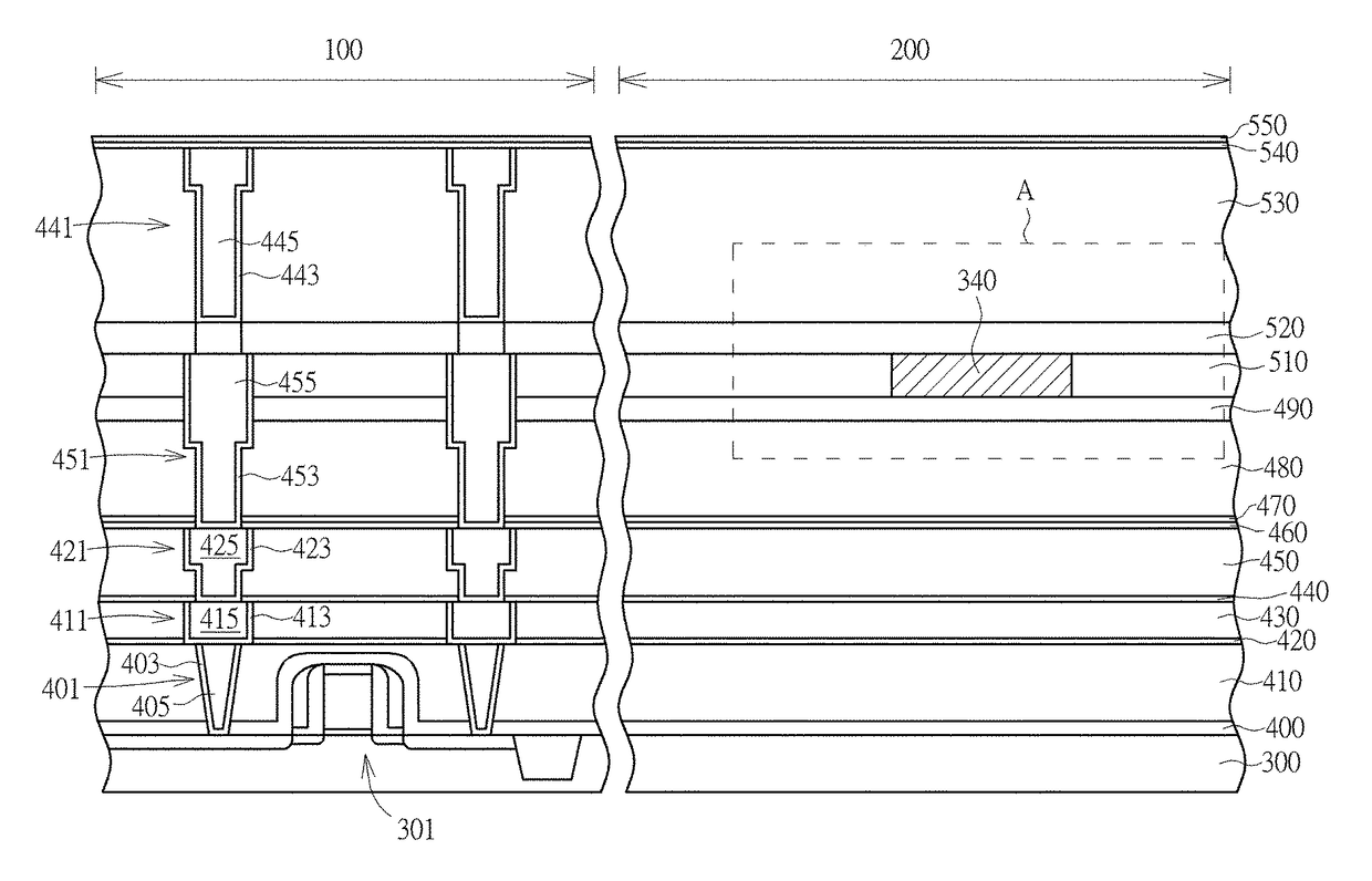
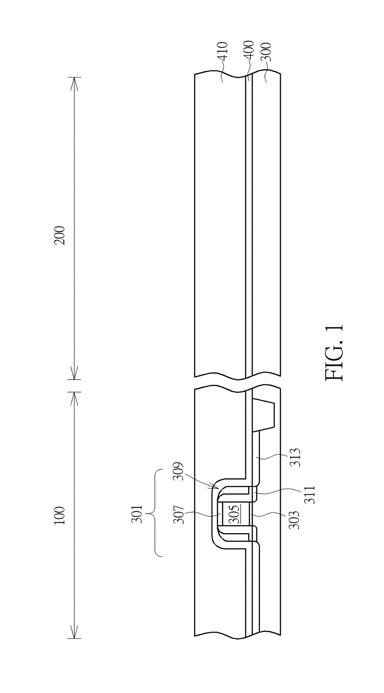
[0026]Please refer to FIG. 1 to FIG. 10, showing schematic diagrams of the method of forming a semiconductor structure according to the present invention. Firstly, a substrate 300 is provided, and which may be any component that can serve as a base for forming devices, like a semiconductor substrate for example, such as silicon substrate, epitaxial silicon substrate, or silicon on insulator (SOI), but is not limited thereto. Also, the substrate 300 includes a first region 100 and a second region 200.

[0027]At least one transistor 301 is formed on the substrate 300, and a contact etch stop layer (CESL) 400 and an interlayer dielectric (ILD) layer 410 are formed on the substrate 300, to cover the transistor 301 and the substrate 300. Precisely, the transistor 301 is formed in the first region 100 of the substrate 300, and includes a gate dielectric layer 303, a gate electrode 305, a capping layer 307 a spacer 309, two light doped drain regions 311 and two source / drain regions 313. In o...

second embodiment

[0049]According to the above description, the semiconductor device according to the present invention is provided. In other words, the present invention further forms a plug structure, and a hydrogen blocking layer disposed thereon, after forming the metal interconnect structure and the oxide semiconductor structure respectively in two different regions of the substrate. It is noted that, the hydrogen blocking layer in the present embodiment may also be formed on the plug structure disposed over the oxide semiconductor structure, such that, the mist and hydrogen diffused in the device may be further sufficiently blocked, so as to avoid such out-diffusion mist and hydrogen flowing along the metal interconnect structure and affecting the oxide semiconductor device in the subsequent forming processes.

[0050]Please refer to FIG. 12, which is a schematic diagram illustrating a method of forming a semiconductor device according to the third embodiment of the present invention. The formal s...


PUM


Abstract

A semiconductor device and a method of fabricating the same, the semiconductor device includes a substrate, an interconnect structure, and an oxide semiconductor structure. The substrate has a first region and a second region. The interconnect structure is disposed on the substrate, in the first region. The oxide semiconductor structure is disposed over a hydrogen blocking layer, in the second region of the substrate.

Description

BACKGROUND OF THE INVENTION[0001]1. Field of the Invention[0002]The present invention relates to a semiconductor device and a method for forming the same, and more particularly, to a semiconductor device having an oxide semiconductor structure and a method for forming the same.[0003]2. Description of the Prior Art[0004]In the modern society, the micro-processor systems comprising integrated circuits (IC) are ubiquitous devices, being utilized in diverse fields such as automatic control electronics, mobile communication devices and personal computers. With the development of technology and the increase of original applications for electronic products, the IC devices are becoming smaller, more delicate and more diversified.[0005]In a wide variety of materials, indium oxide (In2O3), tin oxide (SnO2) and zinc oxide (ZnO) are generally known transparent conductive oxides. Indium tin oxide (ITO), when being formed of a thin film, can be used as a transparent electrode in a flat panel disp...

Claims


Application Information

Patent Timeline
IPC IPC(8): H01L29/78H01L29/786H01L29/66
CPCH01L29/7869H01L29/78696H01L29/66969H01L21/76841H01L23/5329H01L2221/1073H01L27/1225H01L27/124H01L29/4908H01L29/78648
Inventor HSU, CHIA-FUWU, CHUN-YUANSHEN, XU YANGZHOU, ZHIBIAOXING, QINGGANG
Owner UNITED MICROELECTRONICS CORP
Why Eureka
Try Eureka