
Method and system for improving integrated circuit manufacturing productivity

a technology for manufacturing productivity and integrated circuits, applied in the field of integrated circuit design, can solve problems such as problems such as problems in actual checking of design to these two sets of rules, and achieve the effect of improving the manufacturing productivity of integrated circuits

Inactive Publication Date: 2006-07-11
IBM CORP
View PDF2 Cites 23 Cited by
  • Summary
  • Abstract
  • Description
  • Claims
  • Application Information

AI Technical Summary

Benefits of technology

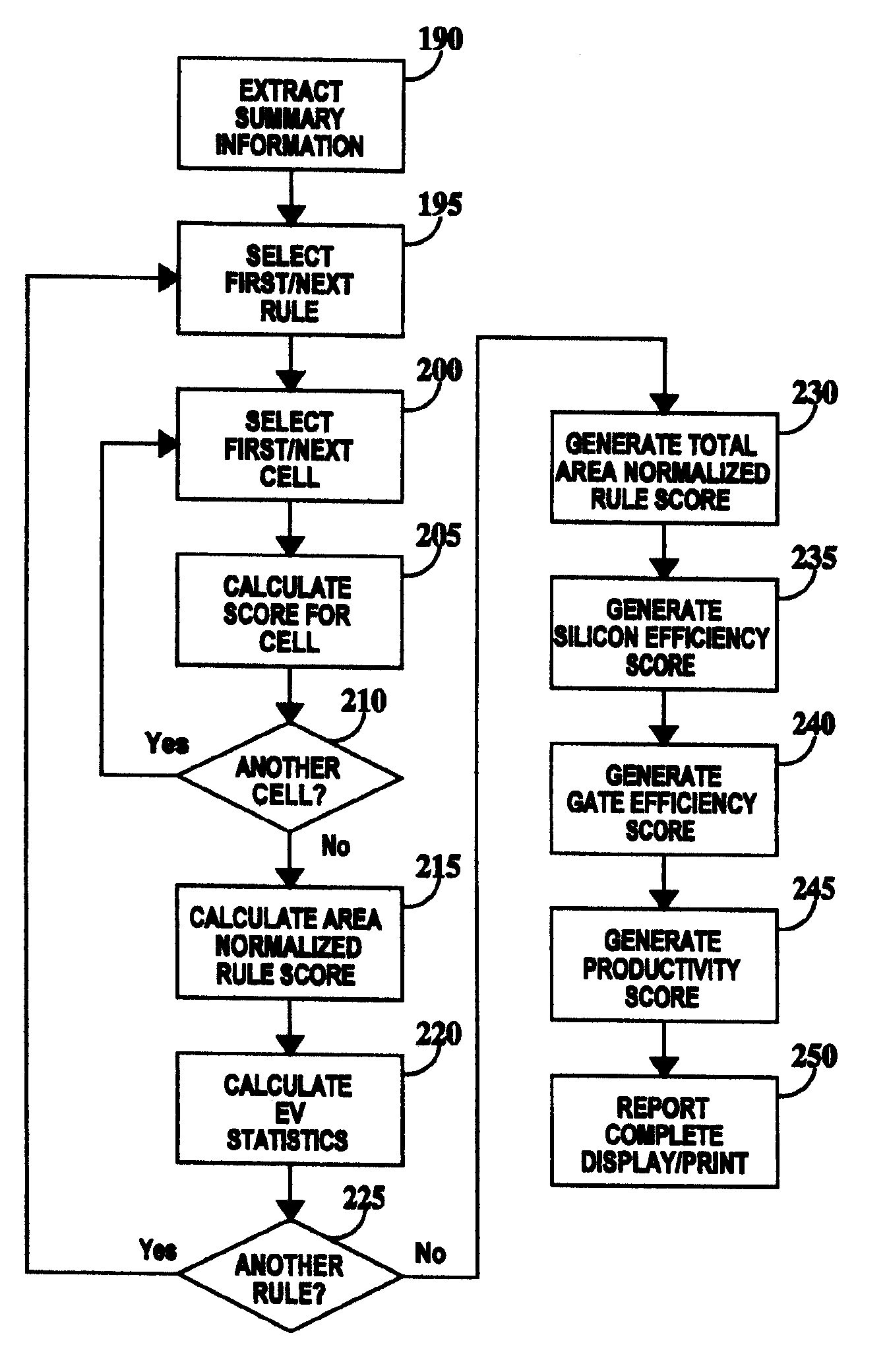
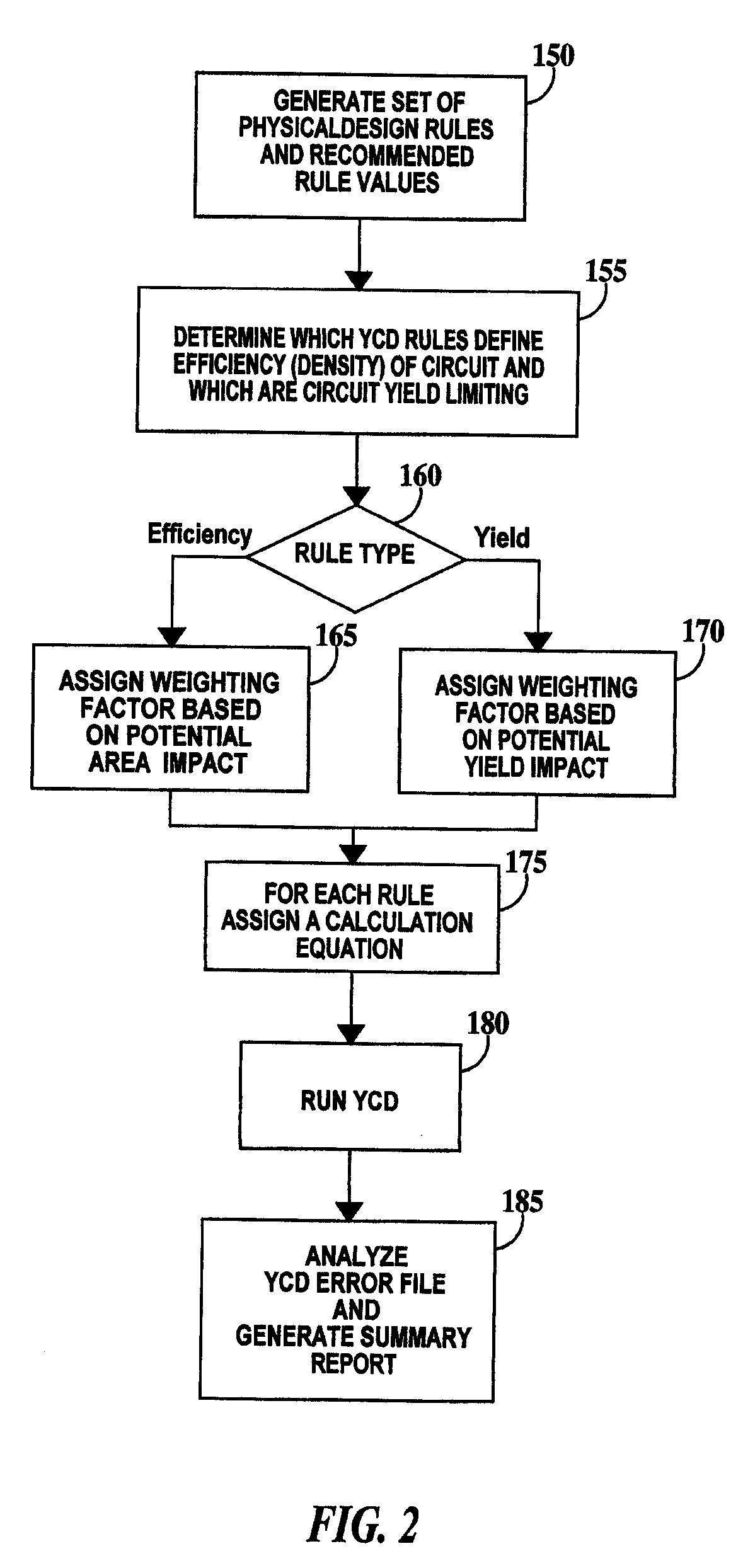
[0005]A first aspect of the present invention is a method of improving manufacturing productivity of an integrated circuit, comprising: (a) generating a set of physical design rules, (b) assigning a rule scoring equation to each physical design rule of the set of physical design rules; (c) checking a physical design of the integrated circuit for deviations from each design rule; (d) computing a score for each physical design rule, using the corresponding rule scoring equation assigned to each physical design rule, for which one or more deviations were found in step (c); and (e) computing a productivity score for the integrated circuit design based on the scores computed in step (d).
[0006]A second aspect of the present invention is A computer system comprising a processor, an address / data bus coupled to the processor, and a computer-readable memory unit coupled to the processor, the memory unit containing instructions that when executed by the processor implement a method for improving manufacturing productivity of an integrated circuit, the method comprising the computer implemented steps of: (a) generating a set of physical design rules, (b) assigning a rule scoring equation to each physical design rule of the set of physical design rules; (c) checking a physical design of the integrated circuit for deviations from each design rule; (d) computing a score for each physical design rule, using the corresponding rule scoring equation assigned to each physical design rule, for which one or more deviations were found in step (c); and (e) computing a productivity score for the integrated circuit design based scores computed in step (d).

Problems solved by technology

Actually checking a design to these two sets of rules is problematic.

Method used


Image

  • Method and system for improving integrated circuit manufacturing productivity
  • Method and system for improving integrated circuit manufacturing productivity
  • Method and system for improving integrated circuit manufacturing productivity

Examples


Embodiment Construction

[0014]The term integrated circuit is intended to include the range from an entire integrated circuit chip through individual integrated circuit functions, such as microprocessors and embedded memory to individual analog and logic circuits.

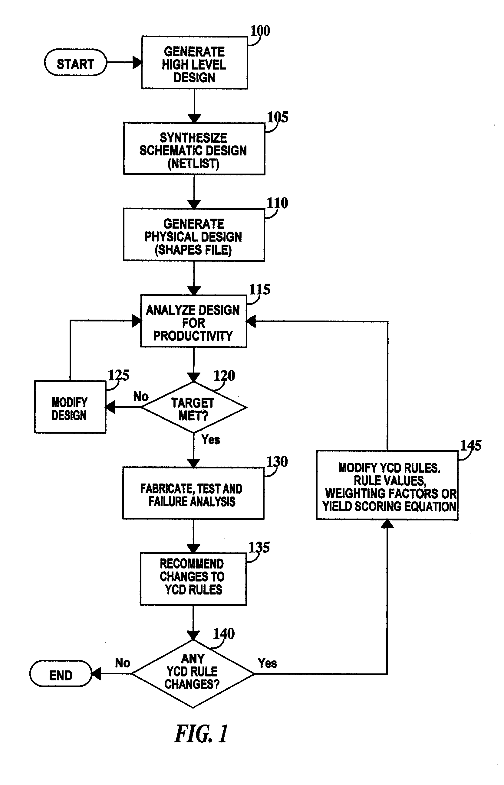
[0015]FIG. 1 is a flowchart illustrating the method of generating and rule checking an integrated circuit design according to the present invention. In step 100, a high-level integrated circuit design is generated. In step 105 the high-level integrated circuit design generated in step 100 is converted into a schematic integrated circuit design (also known as a Netlist) by a synthesis program using circuit elements from a synthesis library. Other activities that may occur in step 105 include, but are not limited to, noise modeling and simulation and timing analysis. Several loops of noise modeling, simulation and timing analysis as well as adjustment to the schematic integrated circuit design (i.e. changing elements, wiring runs, power distribution ...


PUM


Abstract

A method and a system for improving manufacturing productivity of an integrated circuit. The method including: (a) generating a set of physical design rules, (b) assigning a rule scoring equation to each physical design rule of the set of physical design rules; (c) checking a physical design of the integrated circuit for deviations from each design rule; (d) computing a score for each physical design rule, using the corresponding rule scoring equation assigned to each physical design rule, for which one or more deviations were found in step (c); and (e) computing a productivity score for the integrated circuit design based on the scores computed in step (d).

Description

BACKGROUND OF INVENTION[0001]1. Field of the Invention[0002]The present invention relates to the field of integrated circuit design; more specifically, it relates to method and system for improving integrated circuit manufacturing productivity during the design of the integrated circuit.[0003]2. Background of the Invention[0004]As groundrules for integrated circuit design decrease, two sets of groundrules for any given groundrule generation have emerged. The first set of groundrules is the traditional minimum groundrules, i.e. minimum linewidth and space. The second set of groundrules is the recommended groundrules. The first set is directed to functionality, the second set to manufacturing yield. Actually checking a design to these two sets of rules is problematic. Therefore, there is a need in the semiconductor industry for a method of improving integrated circuit manufacturing productivity utilizing efficient rule checking.SUMMARY OF INVENTION[0005]A first aspect of the present i...

Claims


Application Information

Patent Timeline
Patent Type & Authority Patents(United States)
IPC IPC(8): G06F17/50
CPCG06F17/5081G06F2217/12G06F30/398G06F2119/18Y02P90/02
Inventor KEMERER, DOUGLAS W.MAYNARD, DANIEL N.TELLEZ, GUSTAVO E.WANG, LIJIANG L.WISSELL, PETER S.
Owner IBM CORP
Learn More