Substrate for use in semiconductor manufacturing and method of making same

Active Publication Date: 2006-09-05
NAT SEMICON CORP
View PDF5 Cites 89 Cited by
  • Summary
  • Abstract
  • Description
  • Claims
  • Application Information

AI Technical Summary

Benefits of technology

[0009]The described substrate panel may be used to efficiently package a number of integrated circuits. A die is mounted on the substrate in each of the device areas and connectors (e.g. bonding wires) are used to electrically connect each die to their associated contacts. A

Problems solved by technology

The drive toward miniaturization presents many challenges for the IC packaging industry.

Method used


Image

  • Substrate for use in semiconductor manufacturing and method of making same
  • Substrate for use in semiconductor manufacturing and method of making same
  • Substrate for use in semiconductor manufacturing and method of making same

Examples


Embodiment Construction

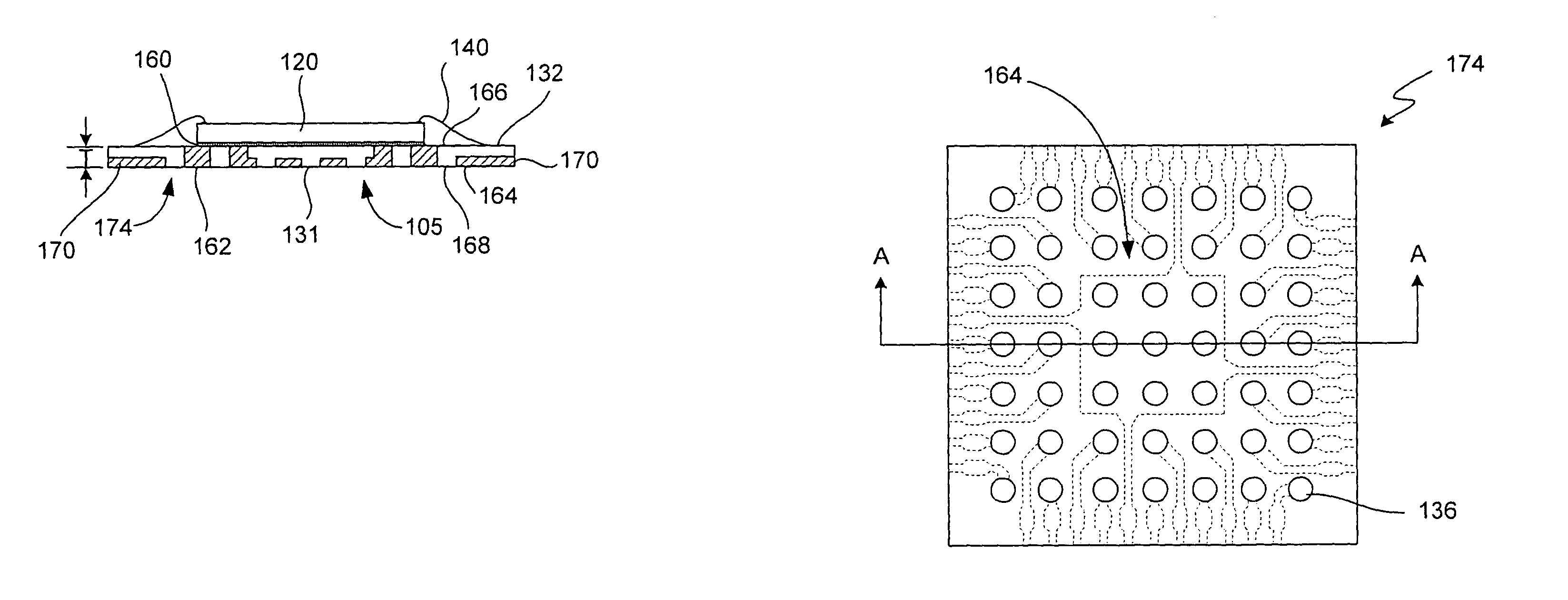
[0024]In one embodiment of the present invention, an improved substrate is described in which portions of the device areas are filled in with a dielectric material. This dielectric material supports the wire bonding landings during wirebonding, eliminating the need for exposed electrically conductive areas that must be covered with insulating strips. It also fills in gaps around the die attach pad, preventing adhesive from flowing into the gaps and eliminating the need to use costly B-stage adhesive.

[0025]This embodiment of the invention is well suited for use in leadless leadframe packages (LLPs), although one of skill will realize that it can be applied to other types of IC packages as well. Thus, the invention should not be construed as being limited to the LLP context. Instead, the invention can be applied to improve any lead-frame in which Support during wirebonding and / or the mitigation of excess die attach adhesive is desirable.

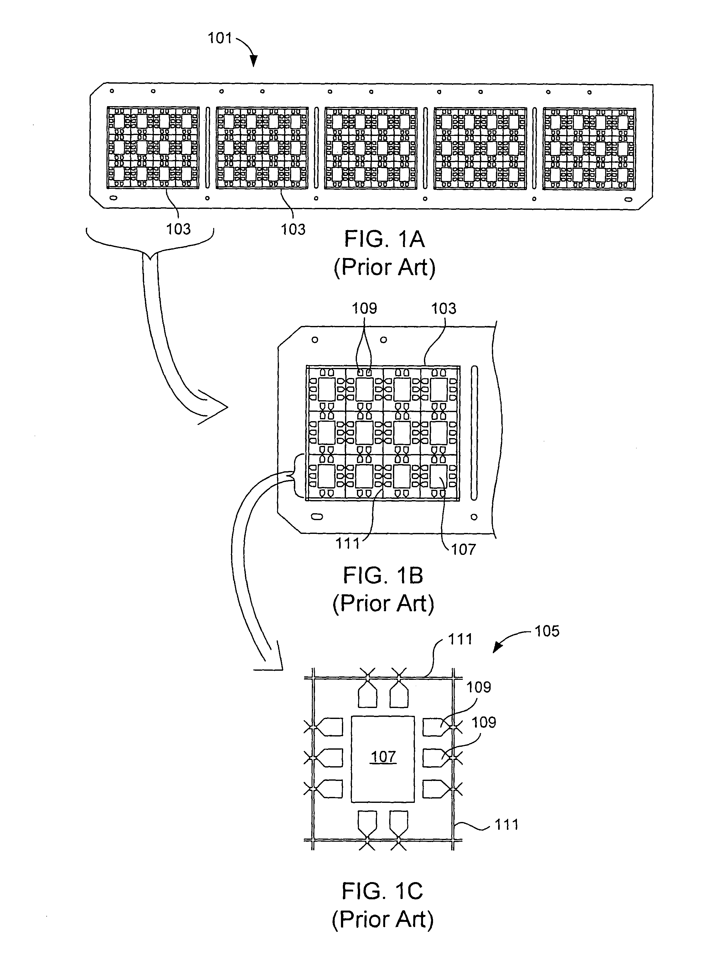
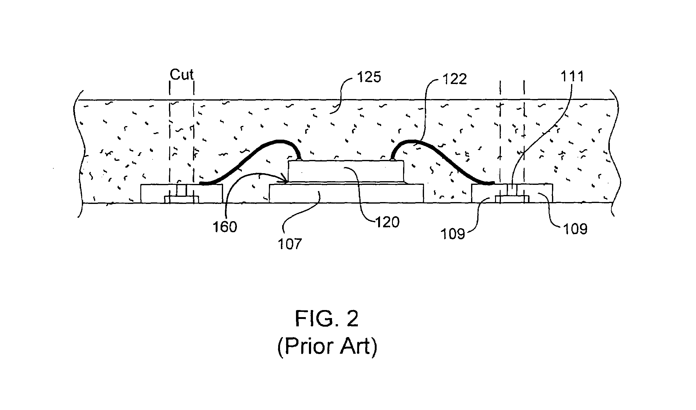
[0026]In co-pending application Ser. No. 09 / 990,...


PUM


Abstract

A lead-frame based substrate panel for use in semiconductor packaging is described. The substrate panel includes a lead-frame panel having at least one array of device areas. Each device area has a plurality of contacts. The lead-frame panel is filled with a dielectric material to form a relatively rigid substrate panel that can be used for packaging integrated circuits. The top surface of the dielectric material is typically substantially coplanar with the top surface of the lead-frame panel, and the bottom surface of the dielectric material is typically substantially coplanar with the bottom surface of the lead-frame panel.

Description

BRIEF DESCRIPTION OF THE INVENTION[0001]This invention relates to the packaging of integrated circuits (ICs). More specifically, this invention relates to substrates for use in IC packaging.BACKGROUND OF THE INVENTION[0002]The drive toward miniaturization presents many challenges for the IC packaging industry. These challenges are partly addressed through use of leadless lead-frame packages (LLPs), which reduce the footprint and height of IC packages by eliminating leads that protrude from the sides of a package, instead employing contacts that are electrically exposed yet lie flush with an outer surface of the package. An LLP is a surface mounted IC package that uses a metal, usually copper, lead-frame substrate to both support the IC die and provide electrical connectivity. As illustrated in FIG. 1A and the successively more detailed FIGS. 1B and 1C, in known LLPs, a copper lead-frame strip or panel 101 is patterned, usually by stamping or etching, to define two dimensional arrays...

Claims


Application Information

Patent Timeline
IPC IPC(8): H01L23/495
CPCH01L23/3107H01L23/49861H01L24/97H01L24/83H01L2224/83H01L2224/32245H01L2224/48465H01L2224/73265H01L2224/97H01L23/49548H01L2924/15747H01L2924/01029H01L2224/48247H01L24/48H01L2224/85H01L2924/00H01L2924/00012H01L24/73H01L2224/49433H01L2924/00014H01L2924/14H01L2924/181H01L2224/45099H01L2224/45015H01L2924/207
Inventor BAYAN, JAIMEPRABHU, ASHOK S.DRUMMOND, FRED
Owner NAT SEMICON CORP
Why Eureka
Try Eureka