Defective pixel specifying method, defective pixel specifying system, image correcting method, and image correcting system

Inactive Publication Date: 2006-09-05
SEMICON ENERGY LAB CO LTD
View PDF43 Cites 54 Cited by
  • Summary
  • Abstract
  • Description
  • Claims
  • Application Information

AI Technical Summary

Benefits of technology

[0035]The present invention is effective for every semiconductor device that has an image sensor function. For example, the present invention is effective for CCD or CMOS type semiconductor devices having an image sensor function, and for any other types of semiconductor devices having an image sensor function as well. The present invention can work effectively in a

Problems solved by technology

Firstly, a subject is not irradiated uniformly with light from a light source in a scanner.
Preferably, calibration sheets are untransmissive, solid and plastic sheets.
As a result, it is very difficult to obtain a semiconductor device having no defective pixel.
A pixel

Method used


Image

  • Defective pixel specifying method, defective pixel specifying system, image correcting method, and image correcting system
  • Defective pixel specifying method, defective pixel specifying system, image correcting method, and image correcting system
  • Defective pixel specifying method, defective pixel specifying system, image correcting method, and image correcting system

Examples


embodiment mode 1

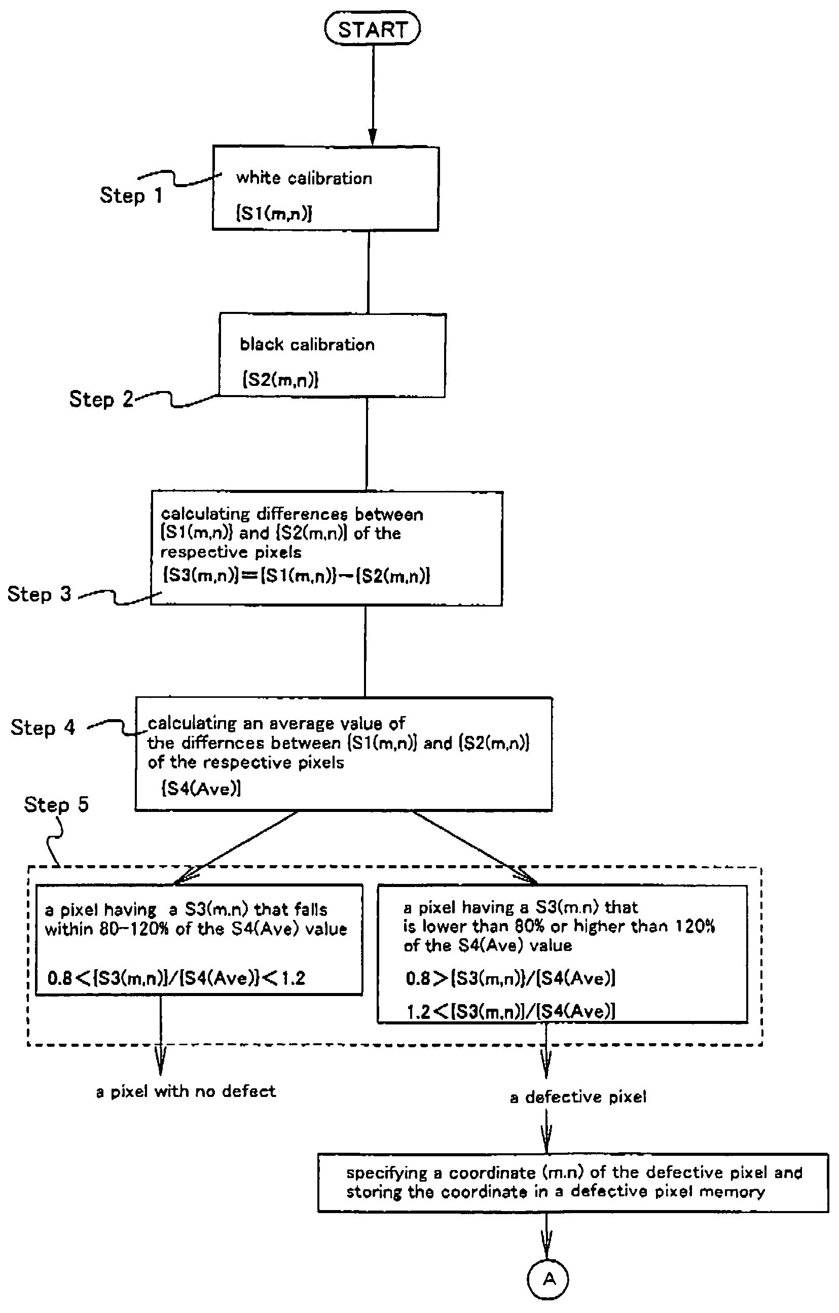
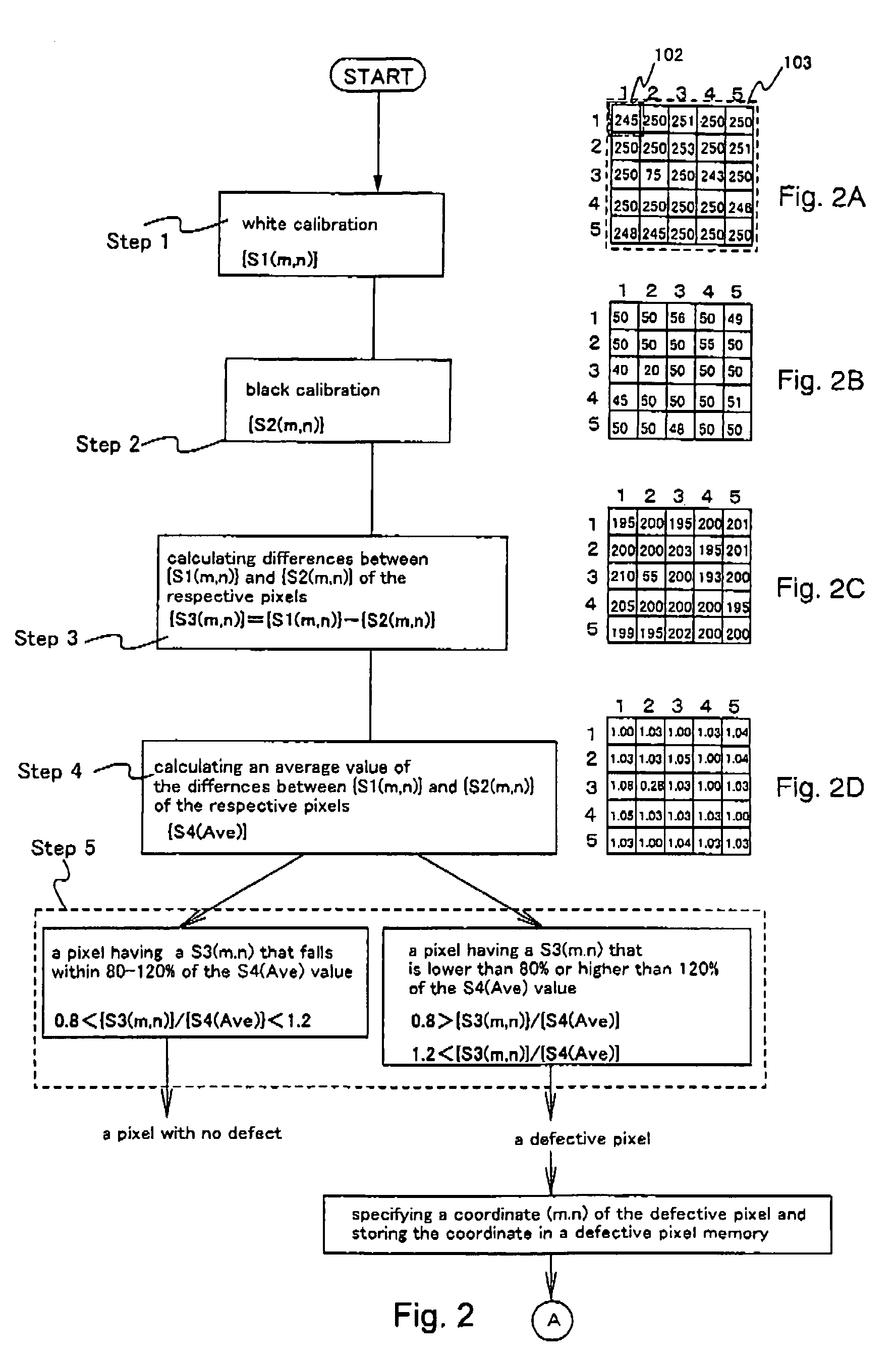
[0058]This embodiment mode describes means for determining whether there is a defective pixel and means for specifying the coordinate of the defective pixel in a defective pixel specifying method of the present invention. The description is given with reference to the flowchart of FIG. 2.

[0059]First, whether or not a pixel portion of a semiconductor device has a defective pixel is determined. The pixel portion reads at least two calibration sheets of different colors to decide. In general, a color is defined by three components; hue (corresponding to the wavelength of a single color light), chroma (vividness, namely, how small the proportion of white is), and brightness (the intensity of light). In this specification, a color may have merely one component or arbitrarily-selected two components out of the above three components. Step 1 of this embodiment consists of reading a white calibration sheet and Step 2 consists of reading a black calibration sheet. Step 3 involves obtaining t...

embodiment mode 2

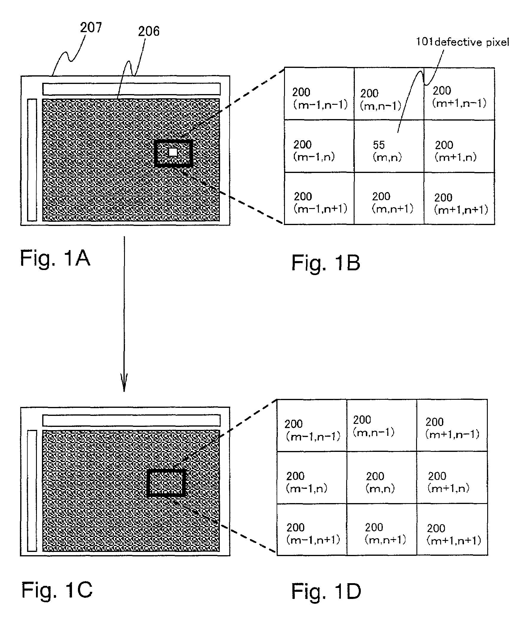
[0072]This embodiment mode describes means for setting an image signal of a defective pixel in an image correcting method of the present invention. The description is given with reference to FIGS. 3A to 3C.

[0073]As shown in FIG. 3A, after the coordinate of a defective pixel 101 is specified and is stored in a defective pixel coordinate memory, an image signal of the defective pixel 101 is set based on image signals of pixels adjacent to the defective pixel.

[0074]FIG. 3B shows a case in which a semiconductor device reads information of a subject in monochrome and displays a monochromatic image of the subject. If the coordinate of the defective pixel 101 is given as (m, n), pixels adjacent to the defective pixel 101 are pixels (m, n±1), pixels (m±1, n±1), and pixels (m±1, n), which are eight pixels in total. An image signal of the defective pixel is set based on image signals of these eight adjacent pixels. To elaborate, the average value of image signals of the pixels (m, n±1), pixel...

embodiment mode 3

[0083]This embodiment mode describes the relation between a pixel portion with a plurality of pixels each having a photoelectric conversion element and a display device for displaying an image of a subject read by the pixel portion. The description is given with reference to FIG. 4.

[0084]In FIG. 4, a pixel portion 200 is provided with a photoelectric conversion element having a reading function. Information of a subject read by the pixel portion 200 is outputted to a defective pixel repairing system. In this embodiment mode, a defective pixel specifying system and an image correcting system are collectively called a defective pixel repairing system.

[0085]The defective pixel repairing system has a CPU 202, an image signal repairing circuit 203, and a defective pixel coordinate memory 204. The defective pixel repairing system of the present invention has means for determining whether there is a defective pixel in the pixel portion through calibration and for specifying the coordinate ...


PUM


Abstract

A defective pixel specifying method and a defective pixel specifying system for a semiconductor device having a defective pixel are provided. Also provided are an image correcting method and an image correcting system for making a defective pixel inconspicuous on the screen when a read image is displayed. The present invention determines whether or not there is a defective pixel for each pixel and specifies the coordinate of the defective pixel using image signals obtained by reading a plurality of images. The image signal of the defective pixel is set based on the image signals of the pixels adjacent to the defective pixel to correct the image of the subject read.

Description

BACKGROUND OF THE INVENTION[0001]1. Field of the Invention[0002]The present invention relates to a defective pixel specifying method and a defective pixel specifying system for a semiconductor device having an image sensor function. The present invention also relates to an image correcting method and an image correcting system for an image read by a semiconductor device having an image sensor function.[0003]2. Description of the Related Art[0004]Various kinds of sensors are developed and put into practice accompanying technology advancement of late. These sensors are used mainly to convert text and image information on paper into data for personal computers. Most of those sensors are semiconductor devices having an image sensor function.[0005]Examples of the above semiconductor devices include digital still cameras, scanners, and copying machines. Digital still cameras are used as replacements for conventional silver film cameras, and have area sensors in which pixels are arranged t...

Claims


Application Information

Patent Timeline
IPC IPC(8): H04N9/64G06T1/00H04N1/40H04N5/217H04N5/335H04N5/367H04N5/369H04N5/372H04N5/374H04N5/378H04N9/30
CPCH04N9/30
Inventor KIMURA, HAJIME
Owner SEMICON ENERGY LAB CO LTD
Why Eureka
Try Eureka