Method for determining fringing capacitances on passive devices within an integrated circuit

a passive device and integrated circuit technology, applied in the field of software tools, can solve the problems of more difficult generation of analytical equations for fringing and mutual capacitance, and problems in numerical convergence accuracy and stability

Inactive Publication Date: 2006-09-05
IBM CORP
View PDF2 Cites 8 Cited by
  • Summary
  • Abstract
  • Description
  • Claims
  • Application Information

AI Technical Summary

Problems solved by technology

Although area capacitance calculations are usually quite straight-forward, the generation of analytical equations for fringing and mutual capacitances tends to be more difficult.
There are many drawbacks associated with the prior art methods of calculating fringing capacitance.
For example, polynomial-based fringing capacitance equations are not always physically based; thus, the initial errors in polynomial fitting procedure can be relatively large, which may cause problems in accuracy and stability of a numerical convergence, etc.

Method used


Image

  • Method for determining fringing capacitances on passive devices within an integrated circuit
  • Method for determining fringing capacitances on passive devices within an integrated circuit
  • Method for determining fringing capacitances on passive devices within an integrated circuit

Examples


application examples

III. APPLICATION EXAMPLES

Example 1

Single-wire Microstrip Transmission Line

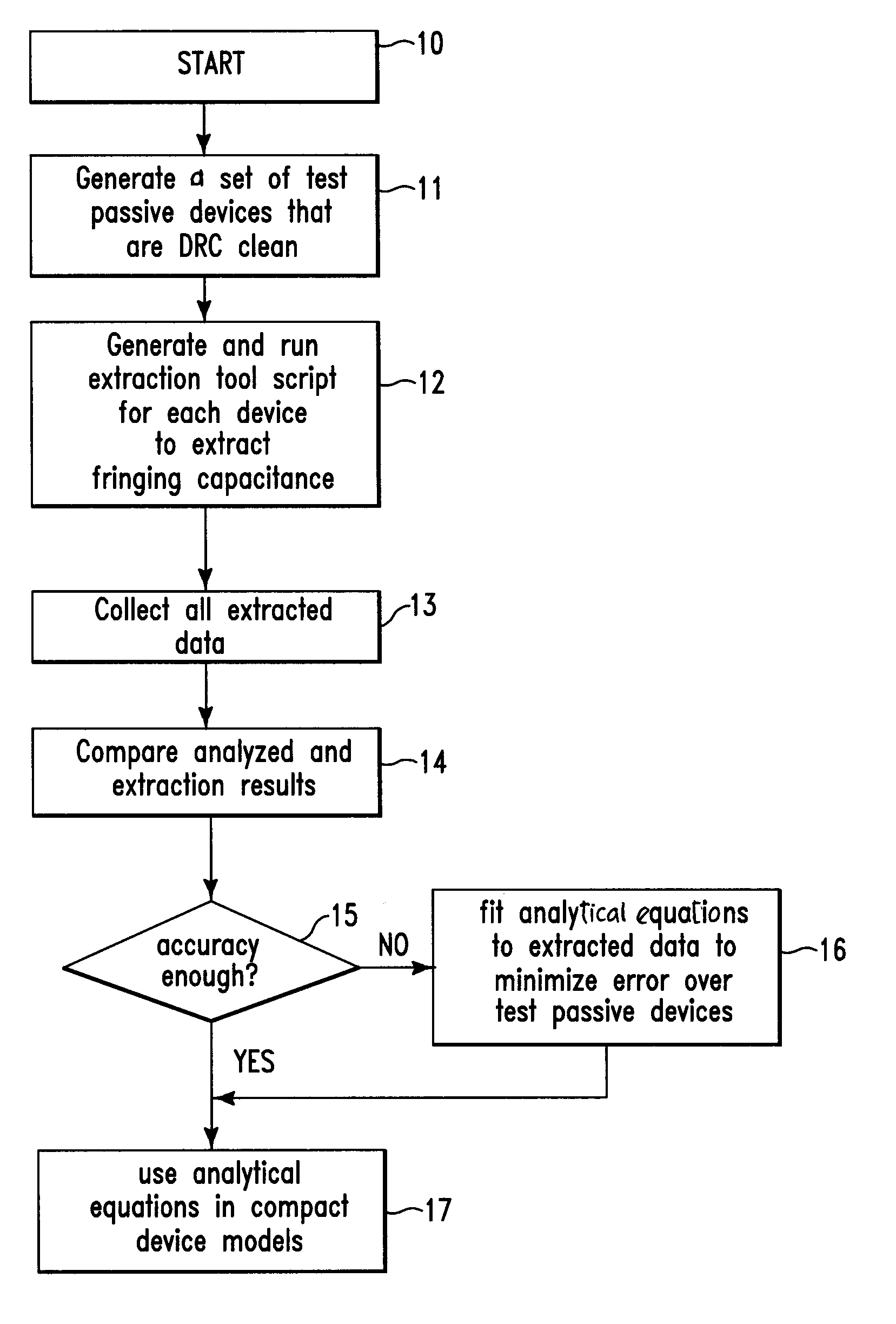
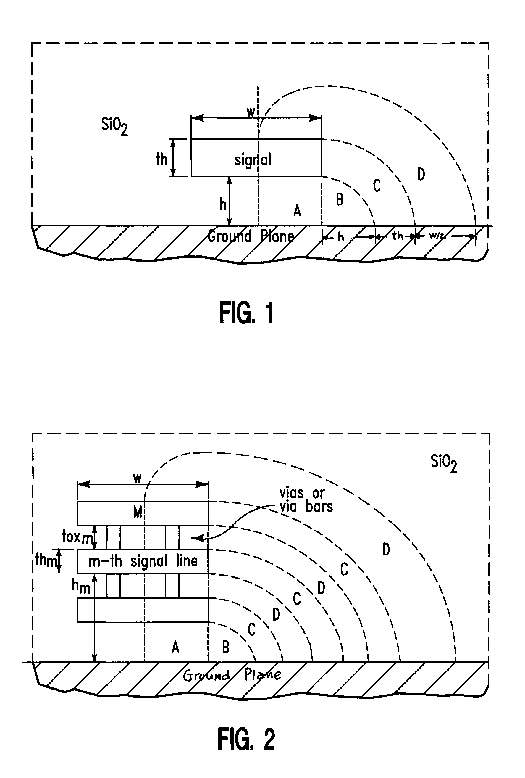
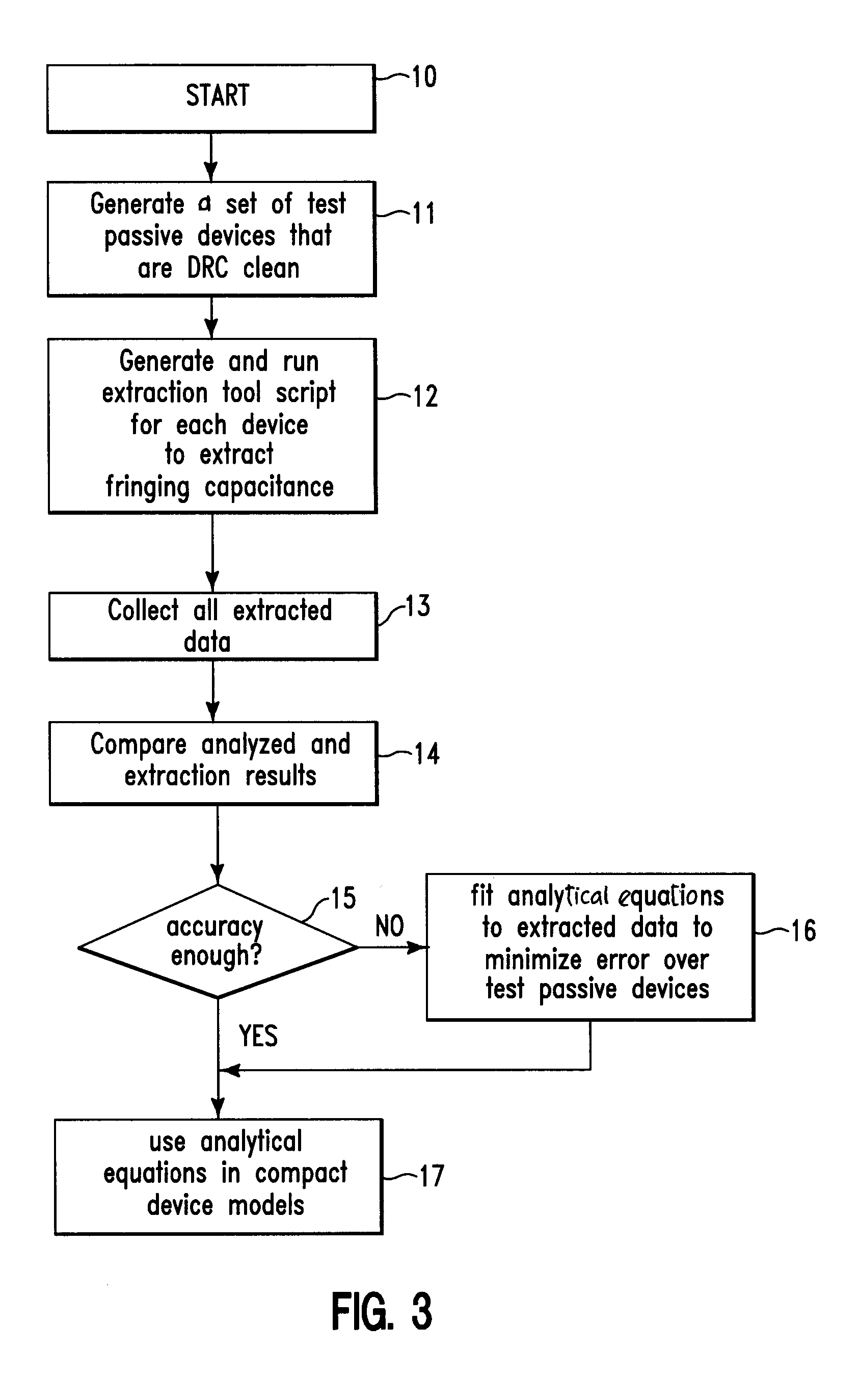
[0041]The capacitances for a single-wire microstrip transmission line includes two parts, namely, area and fringing capacitances. The area capacitance can be calculated using equation (1). After an analytical capacitance equation has been developed, the fringing capacitance can be determined using the methodology shown in FIG. 3.

[0042]The verification results of the analytical capacitance equation is shown in FIG. 4. According to the methodology in FIG. 3, an extraction software (such as QuickCap™) is initially used to generate a large capacitance (area+fringing) database. Then, the obtained database and equations (1) and (5) are utilized to check the accuracy of the initial analytical capacitance equation. As shown in FIG. 4, the maximum error for the analytical fringing capacitance equation is approximately 9%. The extracted capacitance database is also checked against the well-known capacitance calculation ...

example 2

Multi-layer Single Wire Located Above An Infinite Ground Plane

[0046]In production, the infinite ground plane for the multi-layer (stacked) RF_line device configuration as shown in FIG. 2 is actually a silicon substrate. The accuracy of equation (7) versus the number of metal layers from which R_line is constructed is verified. In the present example, the fringing capacitance of interest is due to the electric field in SiO2 at low frequency when the silicon substrate behaves as a good electric conductor. Table I shows the results (per unit length) of numerical comparison using IBM CZ2D fringing capacitance data and the results obtained using equation (7) for a specific process technology.

[0047]

TABLE ICfringingCfringingnumber ofwidthIBM CZ2Dequation 7errorlayers(um)(10−10 F / m)(10−10 F / m)(%)12.00.992480.963752.8922.01.156731.102874.6632.01.262284.353724.3542.01.338681.291483.5352.01.397201.362162.5162.01.443651.423181.4272.01.481431.476910.3182.01.512771.512770.8092.01.539601.568371.87...


PUM


Abstract

A method for detemiining fringing capacitances on passive devices within an integrated circuit is disclosed. A fringing capacitance region on a passive device is initially divided into a group of fringing electric field areas. A set of fringing capacitance equations is then developed for the fringing electric field areas accordingly. A determination is made as to whether or not an accuracy of the fringing capacitance equations meets a predetermined threshold. If so, then the fringing capacitance equations are utilized in compact device models to determine fringing capacitance on the passive device; otherwise, the physically-based fringing capacitance equations are fitted to a set of extracted data to generate a refined set of physically-based fringing capacitance equations, and the refined set of physically-based fringing capacitance equations is utilized in compact device models to determine fringing capacitance on the passive device.

Description

BACKGROUND OF INVENTION[0001]1. Technical Field[0002]The present invention relates to software tools in general, and, in particular, to a method within a software tool for verifying integrated circuit designs. Still more particularly, the present invention relates to a method within a software tool for determining fringing capacitances on single-layer and multi-layer on-chip passive devices.[0003]2. Description of Related Art[0004]On-chip passive devices can have a single or multiple back-end of the line (BEOL) metal layers. Currently, some foundry offers passive on-chip devices as a part of its design kits. Such passive on-chip devices can be spiral inductors (including multi-layer stacked inductors), transmission lines (microstrip and co-planar waveguide inter-connects including stacked metal line over a silicon substrate), bond pads and capacitors (MIM and vertically stacked parallel-plate). Each passive device is supported by schematic symbol, layout parameterized cell (Pcell), ...

Claims


Application Information

Patent Timeline
Patent Type & Authority Patents(United States)
IPC IPC(8): G01R27/00
CPCG06F17/5036G06F30/367
Inventor GOREN, DAVIDKATZENSTEIN, JOHNTRETIAKOV, YOURI V.
Owner IBM CORP
Why Eureka
Try Eureka