Electronic assembly/system with reduced cost, mass, and volume and increased efficiency and power density

a technology of electronic assembly and electronic components, applied in the field of electronic optical packages, can solve the problems of limited brightness, limited display ability, and limited resolution of displays

Inactive Publication Date: 2006-09-12
DISPLAY VECTORS LLC
View PDF32 Cites 31 Cited by
  • Summary
  • Abstract
  • Description
  • Claims
  • Application Information

AI Technical Summary

Benefits of technology

[0003]Large-scale LED displays are typified by the use of T 1 3 / 4 (5 mm) packaged LEDs soldered to rigid printed circuit boards. Such circuit board / modules typically contain a large number of LEDs and must be replaced to correct for the failure of even a single LED. In addition to cost, weight and volume issues or problems, these displays are limited in resolution as a result of the LED package size (typically 0.2 inches in diameter), or about 300 times the plan form area of a bare LED (8000 times the volume), and they are limited in brightness by the small number of LEDs that can be placed in a given area, and also by the thermal resistance of the package and module design. The resolution limit is a function of spacing that is further restricted by package (LED) size. The brightness limit is a function of the number of LEDs per unit area and their individual light output, which is further dependent on the thermal resistance between the LED junction and the local environment. Also, existing LED signage and displays have limited ability to tailor the radiation emission pattern to the needs of the target / audience and thereby increase efficiency. Increased efficiency allows for reduced system and operating cost and / or more radiation delivered to the target.
[0010]An exemplary embodiment of the improved apparatus provides an LED supporting means, such as a grid characterized by ease of conformance to selected shape, curvature, or complex configuration after the LED array is attached to the grid, the grid having flexibility to enable such compliance to desired shaping.
[0013]ii) a superstrate associated with the screen and LEDs to provide structural strength to the assembly.

Problems solved by technology

In addition to cost, weight and volume issues or problems, these displays are limited in resolution as a result of the LED package size (typically 0.2 inches in diameter), or about 300 times the plan form area of a bare LED (8000 times the volume), and they are limited in brightness by the small number of LEDs that can be placed in a given area, and also by the thermal resistance of the package and module design.
Also, existing LED signage and displays have limited ability to tailor the radiation emission pattern to the needs of the target / audience and thereby increase efficiency.
There is need for improvements in LED display assemblies that overcome problems of heating and inability to adequately transfer or dispose of heat generated by LED operation; problems of inadequate LED support on substrates or circuit boards; problems resulting from lack of flexibility of the LED support means; difficulties in manufacturing close packed LED displays; and other problems and difficulties as will appear.

Method used


Image

  • Electronic assembly/system with reduced cost, mass, and volume and increased efficiency and power density
  • Electronic assembly/system with reduced cost, mass, and volume and increased efficiency and power density
  • Electronic assembly/system with reduced cost, mass, and volume and increased efficiency and power density

Examples


Embodiment Construction

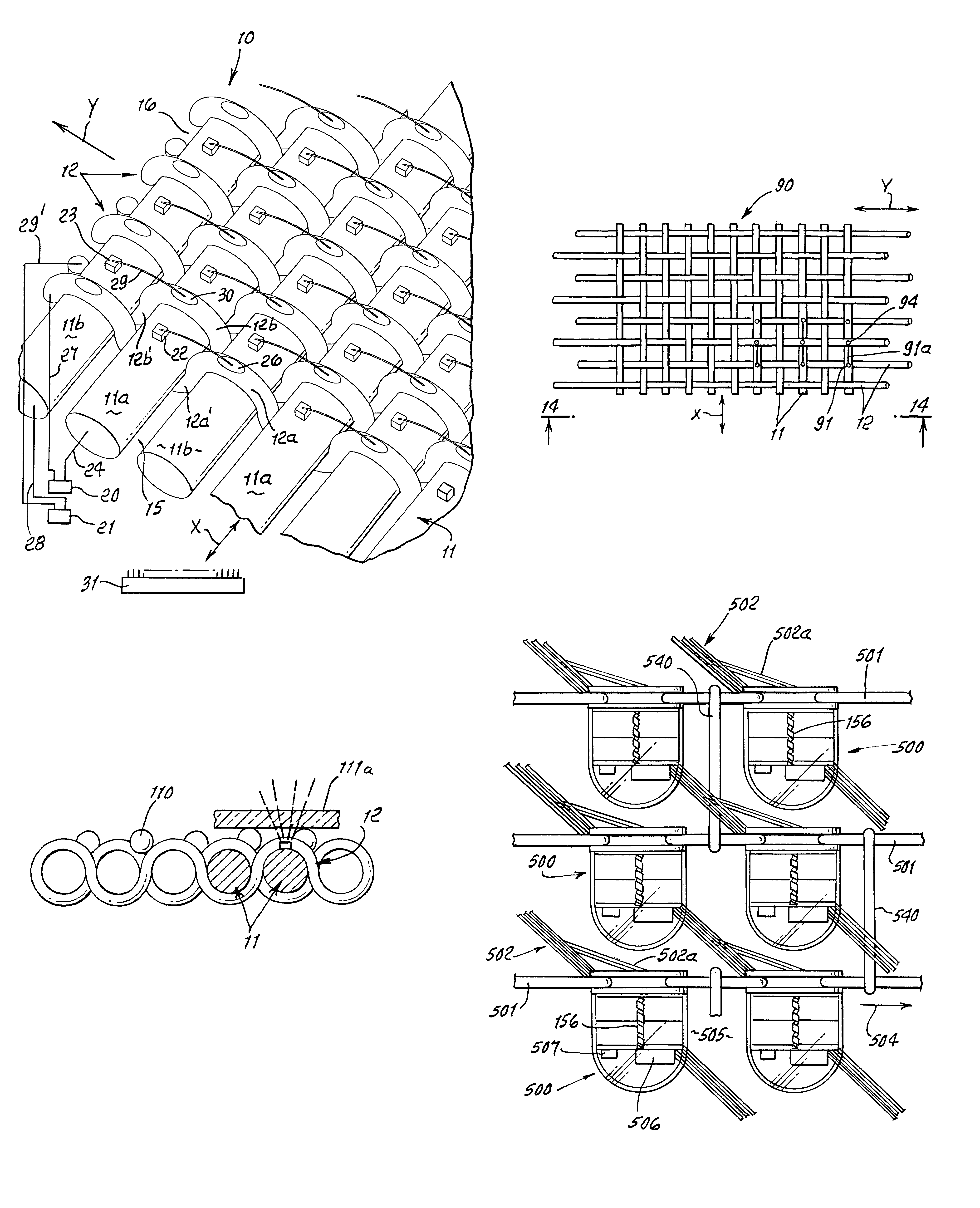
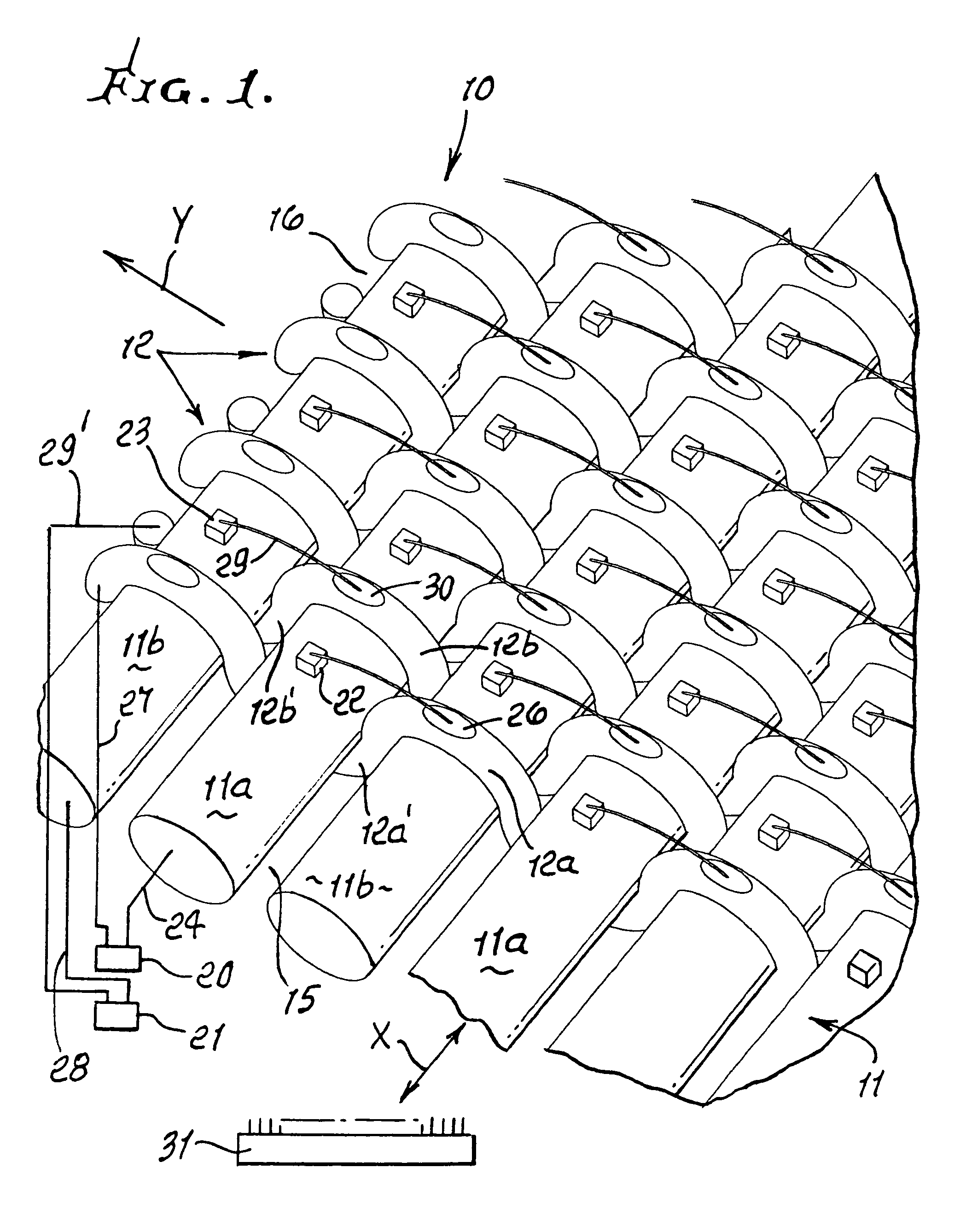
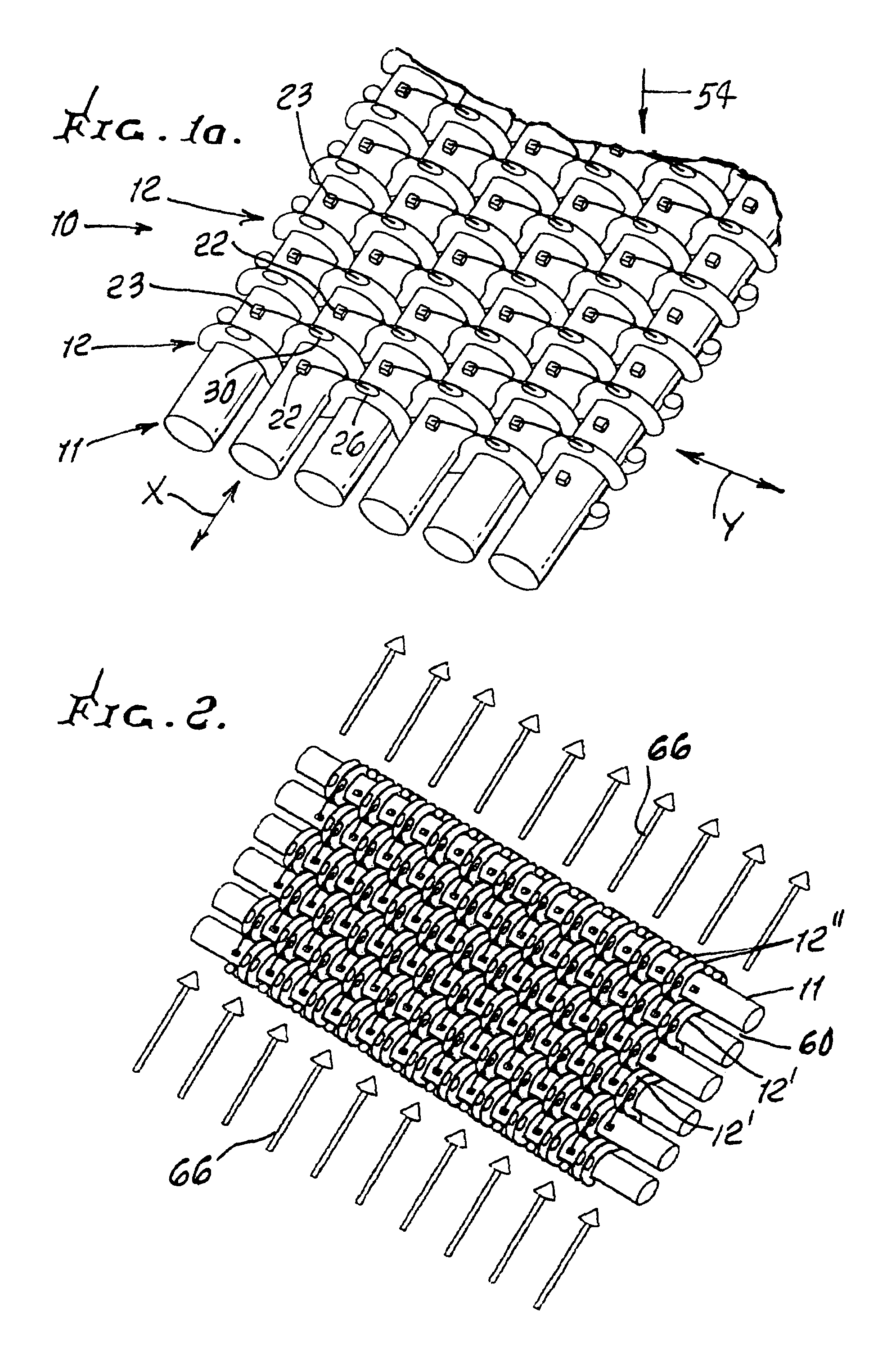
[0072]FIG. 1 shows a screen 10 forming a grid of electrical conductors. As illustrated, the conductors include like primary conductors 11 extending generally in one direction, and designated as an X-direction; and secondary conductors 12 extending generally in another direction, designated as a Y-direction. As shown, the primary conductors preferably have overall diameters d1 or cross sections greater than the overall diameters d2 or cross sections of the secondary conductors, and the latter extend over and under the conductor 11 in a weaving or mesh relationship as at 12a and 12a′. There is space as at 15 between successive parallel conductors 11; and there is space as at 16 between successive undulating conductors 12, whereby coolant can flow downwardly through the screen via spaces 15 and 16 and near or adjacent diodes, to remove heat generated by diode operation.

[0073]Light emitting diodes are located or mounted in an array on various conductors, as shown on crests of conductor ...


PUM

PropertyMeasurementUnit
anglesaaaaaaaaaa
diameteraaaaaaaaaa
electricalaaaaaaaaaa

Abstract

An LED display assembly, comprising a grid of electrical conductors; light emitting diodes in association with the grid and in electrical communication with the conductors that provide power for LED operation, the grid operable to receive heat from the diodes during diode operation, and the array configured for passing coolant fluid for transfer of heat to the fluid. LED packages adjustable relative to a mounting grid, are also provided.

Description

BACKGROUND OF THE INVENTION[0001]This application claims priority over provisional application Ser. No. 60 / 405,826 filed Aug. 26, 2002.[0002]The apparatus described and claimed herein relates generally to electronic-optical packages, and more particularly to grids or arrays of such packages supported in such manner as to facilitate their installation and use as in closely assembled or packed configurations. Provisional application Ser. No. 60 / 405,826 is incorporated herein by reference.[0003]Large-scale LED displays are typified by the use of T 1 3 / 4 (5 mm) packaged LEDs soldered to rigid printed circuit boards. Such circuit board / modules typically contain a large number of LEDs and must be replaced to correct for the failure of even a single LED. In addition to cost, weight and volume issues or problems, these displays are limited in resolution as a result of the LED package size (typically 0.2 inches in diameter), or about 300 times the plan form area of a bare LED (8000 times th...

Claims


Application Information

Patent Timeline
Patent Type & Authority Patents(United States)
IPC IPC(8): H01L29/18H01L23/02H01L23/34H01L23/52H01L33/00G09F9/33H01L25/075H01L33/62H01L33/64
CPCD03D1/0088D03D15/00D03D15/0083D03D15/02G09F9/33D03D9/00H01L2224/48091D10B2101/20D10B2401/16H01L25/0753H01L33/62H01L33/648H01L2224/45147H01L2924/01015Y10S257/91H01L2224/45124H01L2924/3025H01L2924/00H01L2924/00014H01L2224/45015H01L2924/00011D03D15/67H01L2924/207H01L2924/01033F21K9/00
Inventor POPOVICH, JOHN M.
Owner DISPLAY VECTORS LLC
Why Eureka
Try Eureka