Method for manufacturing finFET

a transistor and field effect technology, applied in the direction of semiconductor devices, electrical equipment, basic electric elements, etc., can solve the problems of inapplicability of current photolithography process technology to the exposure of photoresist patterns with a pitch less than 78 nm, difficult to shrink the device's size, and inability to increase the density of fin-shaped structures

Active Publication Date: 2015-09-22
UNITED MICROELECTRONICS CORP
View PDF2 Cites 16 Cited by
  • Summary
  • Abstract
  • Description
  • Claims
  • Application Information

AI Technical Summary

Benefits of technology

[0005]Here, a method for manufacturing a fin field-effect transistor (FinFET) according to the invention is provided. The method is free of restriction on the resolution limit of the conventional photolithography process, and suitable for manufacturing fin-shaped structures characterized by an integral multiple of pitches and a non-integral multiple of pitches simultaneously.
[0006]In order to achieve the above and other advantages, the invention provides a method for manufacturing a FinFET, comprising: forming a first multi-layer structure and a second multi-layer structure on a substrate sequentially; forming a first sacrificial pattern on the second multi-layer structure, wherein the first sacrificial pattern is composed of a plurality of first mandrels and a second mandrel, and the adjacent first mandrels are separated with a first interval, and the adjacent first and second mandrels are separated with a second interval; forming a first spacer with a first width on a sidewall of the first sacrificial pattern, and forming a merging spacer with a second width between the adjacent first mandrels, wherein the first interval is the same as the second width and less than twice of the first width, and the second interval is larger than twice of the first width; removing the first sacrificial pattern; etching away a portion of the second multi-layer structure, by use of the first spacer and the merging spacer as a hard mask, so that a second sacrificial pattern is formed; forming a second spacer on a sidewall of the second sacrificial pattern; removing the second sacrificial pattern; etching away a portion of the first multi-layer structure, by use of the second spacer as a hard mask, so that the first multi-layer structure is patterned; and etching away a portion of the substrate, by use of the patterned first multi-layer structure as a hard mask, so that a plurality of first fin-shaped structures having a first pitch therebetween and a plurality of second fin-shaped structures having a second pitch therebetween are formed, wherein the first pitch is a non-integral multiple of the second pitch.
[0007]In summary, according to the invention, the intervals existed between the first mandrels and the second mandrels and respective widths of the first mandrels and the second mandrels are purposely modified. The most important is a first interval between the adjacent first mandrels is purposely modified as shorter than twice of thicknesses of a nitride layer, which is subsequently devoted to the first spacer. Therefore, a merging spacer can be generated between the adjacent first mandrels resulted from the union of respective spacers of the adjacent first mandrels, instead of respective spacers of the adjacent first mandrels being separated from each other customarily. Besides, through a plurality of sidewall pattern-transferring processes, it is able to manufacture a FinFET composed of fin-shaped structures characterized by a non-integral multiple of pitches (such as 45 nanometers, as a non-integral multiple of 32 nanometers) as well as an integral multiple of pitches (such as an integral multiple of 32 nanometers). Accordingly, it is possible to overcome the resolution limit of the conventional photolithography process, as well as the restriction of mere integral multiple of pitches, and accomplish various structures of respective functional areas in the device.
[0008]For making the above and other purposes, features and benefits become more readily apparent to those ordinarily skilled in the art, the preferred embodiments and the detailed descriptions with accompanying drawings are set forth in the following descriptions.

Problems solved by technology

However, due to the restriction of a resolution limit of the photolithography process, the current photolithography process technology is not applicable to the exposure of photoresist patterns with a pitch less than 78 nm.
With such a photolithography process technology, it is impossible to increase the density of fin-shaped structures, and difficult to shrink the device's size.
That is to say, the conventional photolithography process technology has failed to fulfill the requirement of various fin-shaped structures of respective functional areas in a device.

Method used


Image

  • Method for manufacturing finFET
  • Method for manufacturing finFET
  • Method for manufacturing finFET

Examples


Embodiment Construction

[0011]The invention will now be described more specifically with reference to the following embodiment. It is to be noted that the following descriptions of the preferred embodiment are presented herein for purpose of illustration and description only. It is not intended to be exhaustive or to be limited to the precise form disclosed.

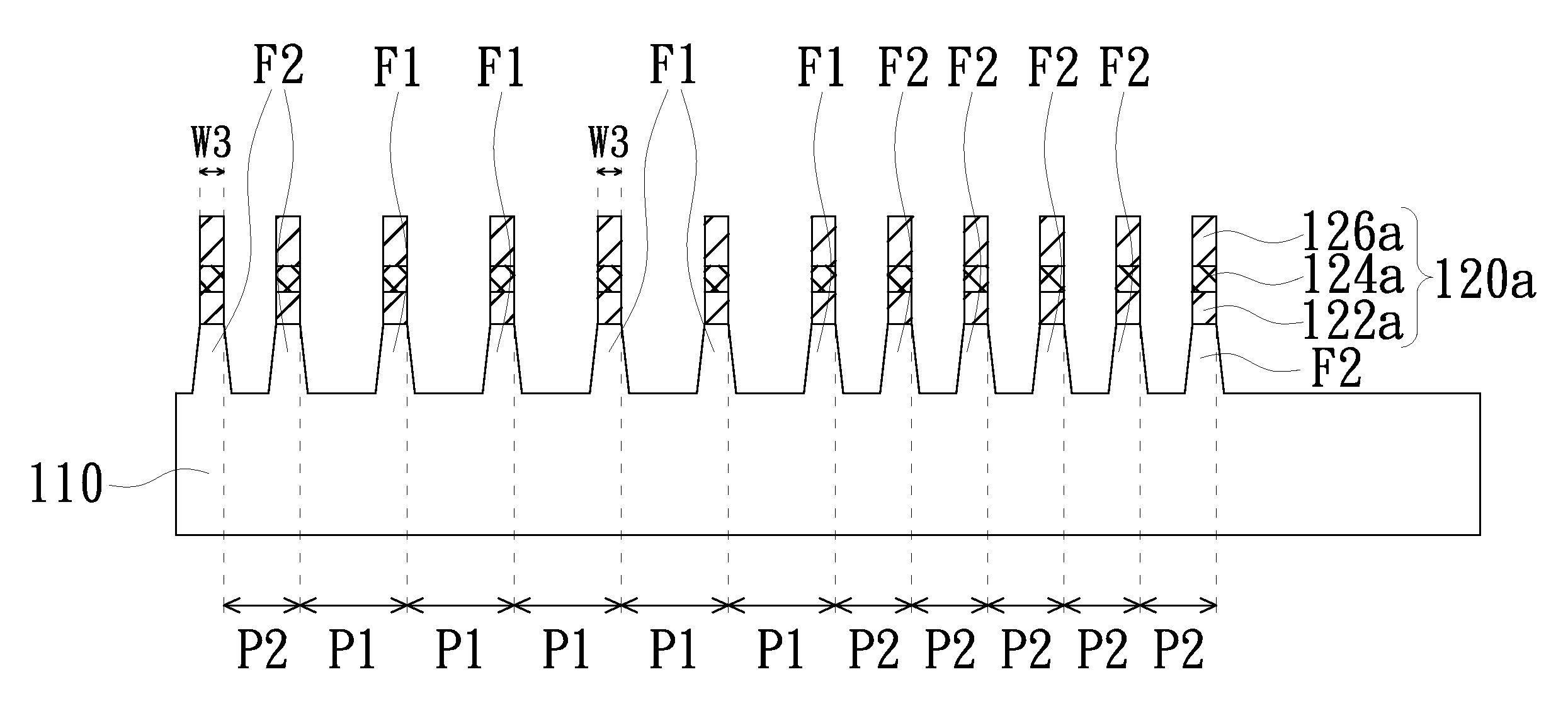
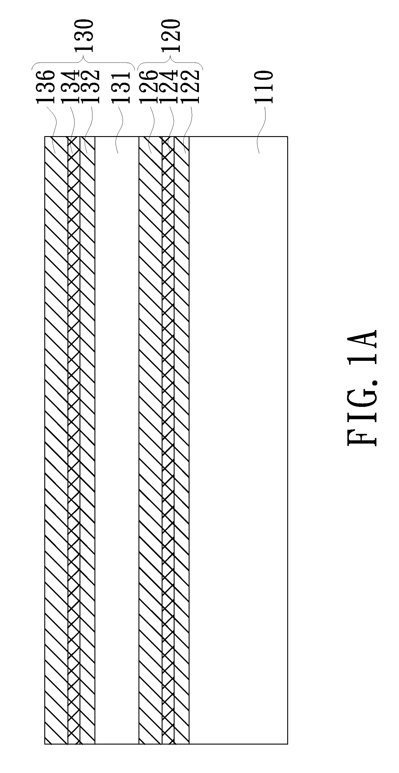
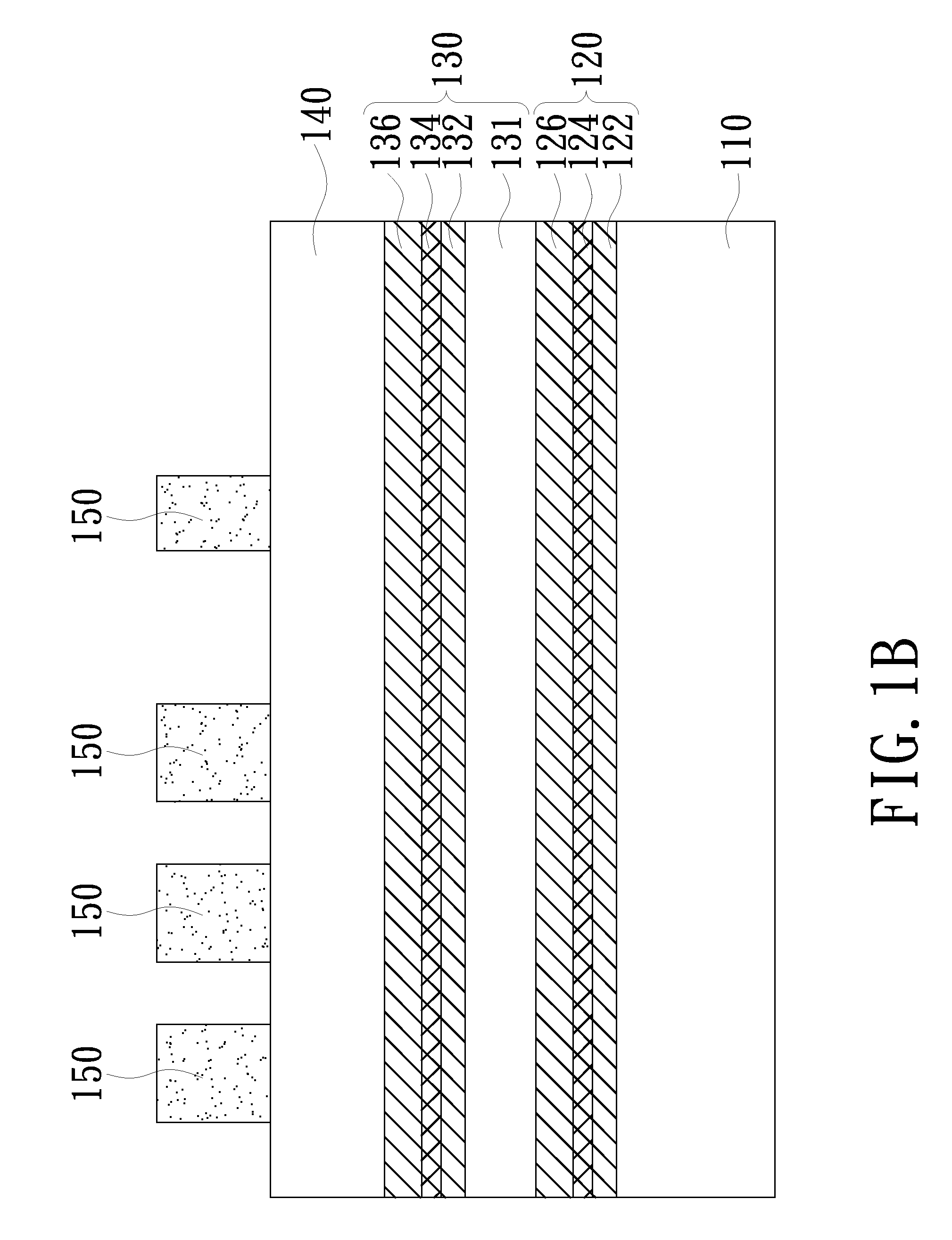
[0012]FIGS. 1A-1N are flowcharts illustrating a method for manufacturing a FinFET according to one embodiment of the invention. Firstly, by referring to FIG. 1A, a method for manufacturing a FinFET according to the embodiment includes providing a substrate 110, wherein the substrate 110 is a silicon substrate or a doped silicon substrate. Next, a stacked multi-layer structure is formed on the substrate 110, for example, a first multi-layer structure 120 and a second multi-layer structure 130 are formed and stacked sequentially on the substrate 110, respectively. Here, both of the first multi-layer structure 120 and the second multi-layer structure 130 a...


PUM


Abstract

A method for manufacturing a FinFET includes forming a merging spacer, through a plurality of sidewall pattern-transferring processes, and modifying a first interval between adjacent first mandrels as shorter than twice of thicknesses of a nitride layer, which is formed on the first mandrels and contoured thereto, followed by a first spacer being formed on a sidewall thereof, so that a FinFET composed of a plurality of fin-shaped structures having a non-integral multiple of pitches as well as an integral multiple of pitches can be manufactured.

Description

FIELD OF THE INVENTION[0001]The invention relates to a method for manufacturing a transistor, and more particularly to a method for manufacturing a fin field-effect transistor (FinFET).BACKGROUND OF THE INVENTION[0002]In the present generation of tremendous advancement of technology, when pursuing the miniaturization of device, it is also necessary to enhance the performance thereof simultaneously. In contrast to a conventional planar field-effect transistor, it is more appropriate for a fin field-effect transistor (hereinafter referred to as FinFET) to dominate the current therethrough, while alleviate the leakage current and dynamic power dissipation. In the trend of the miniaturization of device, the FinFET has been shrunk in a nanometer scale.[0003]However, due to the restriction of a resolution limit of the photolithography process, the current photolithography process technology is not applicable to the exposure of photoresist patterns with a pitch less than 78 nm. With such a...

Claims


Application Information

Patent Timeline
Patent Type & Authority Patents(United States)
IPC IPC(8): H01L21/02H01L21/308H01L21/3105H01L21/311H01L29/66
CPCH01L29/6656H01L21/31116H01L21/31051H01L21/3086H01L21/022H01L29/66795
Inventor LIN, CHAO-HUNGTSAI, SHIH-HUNGFU, SSU-IJENQ, JYH-SHYANG
Owner UNITED MICROELECTRONICS CORP
Why Eureka
Try Eureka